TECH
BRIEF
Capacitance and Signal
Integrity
Csup
RLOAD
VOUT
-
Figure 1. Sample parallel circuit
e
e
VIN
Capacitance is an important device characteristic that is intentionally used in circuit
design. Actually, the use of capacitance is a
common technique for noise filtering. The
parallel capacitor attenuates high frequency
noise, while the circuit operates without
disruption at lower frequencies.
Conversely, a series capacitor will block low
frequencies and pass high frequencies without attenuation or distortion.
Suppressor capacitance is an important
consideration for the Design Engineer since
the suppressors are installed in parallel in
the circuit that is to be protected.
Remembering the capacitor example, as the
speed of a data stream increases, the
amount of distortion that is done will
increase as a function of the device capacitance. As a result, high frequency signals
can be “filtered” due to the capacitance of
the suppressor.
In order to avoid “filtering” or distortion of
the signal, it is necessary to make sure that
Time (t)
ll Tim
+
Why is Capacitance an
Issue?
Before discussing the data, it is necessary to
define the circuit and signals that will be
evaluated. The test circuit is similar to the
previous figure. A signal generator is used
to send the signal at various frequencies, a
capacitor and various suppressors are used
to give various capacitance values, and the
load is represented by a 50Ω resistor.
The signal generator creates a “pulse” that
looks like a single “bit” of digital data. The
width of the pulse and the time between
pulses are varied to change the frequency
of the signal. Here is a look at the signal
(waveform) that will be sent by the generator.
t f - Fa
One of the most “defining” of these characteristics is the capacitance of the device.
Capacitance is an electrical attribute of any
circuit element (resistance would be an
example of another attribute) and is nonlinear with respect to signal frequency. In
other words, as the signal frequency
increases, the capacitance effect (impedance) changes. If a mismatch occurs
between the capacitance of a suppressor
and the signal speed of a circuit, the signal
(and its ability to properly transmit data)
can be degraded.
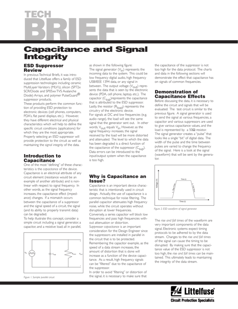
To help illustrate this concept, consider a
simple circuit including a signal generator, a
capacitor, and a resistive load; all in parallel,
Demonstration of
Capacitance Effects
e Tim
Introduction to
Capacitance
the capacitance of the suppressor is not
too high for the data protocol. The charts
and data in the following sections will
demonstrate the effect that capacitance has
on signals of common frequencies.
tr - Ris
In previous Technical Briefs, it was introduced that Littelfuse offers a family of ESD
suppression technologies including ceramic
MultiLayer Varistors (MLV’s), silicon (SP72x
SCR/Diode and SP05xx TVS Avalanche
Diode) Arrays, and polymer PulseGuard®
suppressor products.
These products perform the common function of providing ESD protection to
electronic devices (cell phones, computers,
PDA’s, flat panel displays, etc.). However,
they have different electrical and physical
characteristics which will help to define the
specific circuit conditions (applications) for
which they are the most appropriate.
Properly selecting an ESD suppressor will
provide protection to the circuit as well as
maintaining the signal integrity of the data.
as shown in the following figure:
The signal generator (Vin) represents the
incoming data to the system. This could be
low frequency digital audio, high frequency
USB/IEEE 1394 data, or any signal in
between. The output voltage (Vout) represents the data that is seen by the electronic
device (PDA, cell phone, laptop, etc.). The
capacitor (Csup)represents the capacitance
that is attributed to the ESD suppressor.
Lastly, the resistor (Rload) represents the
circuitry of the electronic device.
For signals at DC and low frequencies (e.g.
audio range), the load will see the same
signal that the generator sent out. In other
words, Vout equals Vin. However, as the
signal frequency increases, the signal
received by the load will be more distorted
and attenuated. The level to which the data
has been degraded is a direct function of
the capacitance of the suppressor (Csup).
Data errors can be introduced to the
input/output system when the capacitance
is too high.
Voltage (V)
ESD Suppressor
Review
Time (t)
Figure 2. ESD waveform of signal generator
The rise and fall times of the waveform are
very important components of the data
signal. Electronic systems expect timing
protocols to be adhered to by the data
stream. Changes to the rise and fall times
of the signal can cause the timing to be
disrupted. By making sure that the capacitance value of the ESD suppressor is not
too high, the rise and fall times can be maintained. This ultimately leads to maintaining
the integrity of the data stream.
Demonstration of
Capacitance Effects
(cont’d).
To demonstrate the effect that capacitance
has on data signals, several devices of different capacitance values were chosen. Then,
different speed signals were run through
the test circuit with these devices inserted
in place of Csup. The waveforms were
captured, and the amount of distortion due
the device capacitance could be seen. The
following devices were used in the tests:
can be compromised if capacitance is not
taken into account.
It is not enough that a suppressor provides
reliable ESD protection, the suppressor
must also be properly selected so that it
maintains data integrity. As data rates
continue to increase, it will be increasingly
important to match the suppressor properly to the application. Suppressors that
protect extremely high speed applications
must have low capacitance values.
Peak to Peak Voltage Amplitude at 480mV
Signal Frequency at 6MHz Equal to 12Mbit/sec
• PulseGuard® suppressor - 0.050pF
(PGB0010603)
• Multilayer Chip Capacitor - 10 pF
• Multilayer Chip Capacitor - 1.0 pF
• Multilayer Varistor - 660 pF
(V5.5MLA0603)
Summary
The purpose in providing this data is to
show that the capacitance characteristic is
an important criterion when choosing an
ESD suppressor. The effectiveness of ESD
suppression technologies is not questioned
here, rather it is noted that signal integrity
Without Device
10.0 pF 0603 Capacitance
1.0 pF 0603
Capacitance
1.0E-01
0.0E+01
-1.0E-01
-2.0E-01
-3.0E-01
1.0E-07
0.0E+00
4.0E-08
1.4E-07
1.8E-07
1.2E-07
6.0E-08
1.6E-07
2.0E-08
2.0E-07
Time (sec)
Figure 3. Capacitive loading effects on USB 1.1 signal.
Peak to Peak Voltage Amplitude at 480mV
Signal Frequency at 240MHz Equal to 480Mbit/sec
Without Device
10.0 pF 0603 Capacitance
PGB0010603
V5.5MLA0603
1.0 pF 0603
Capacitance
3.0E.01
Voltage (V)
2.0E-01
1.0E-01
0.0E+01
-1.0E-01
-2.0E-01
-3.0E-01
0.0E+00
1.0E-09 2.0E-09
3.0E-09
4.0E-09 5.0E-09
1.5E-09
5.0E-10
4.5E-09
2.5E-09 3.5E-09
Time (sec)
Figure 4. Capacitive loading effects on USB 2.0 signal.
Specifications, descriptions and illustrative material in this literature are as accurate as known at time of publication, but are
subject to change without notice. Littelfuse is a registered trademark of Littelfuse Incorporated.
EC624
PGB0010603
V5.5MLA0603
2.0E-01
Voltage (V)
In the first graph, a “low” speed signal was
used. The frequency of the signal approximates the USB 1.1 Full Speed protocol, 12
Mbps. It is seen that the PulseGuard
suppressor and the 1.0 and 10.0 pF capacitors do not affect the original waveform.
However, the 660 pF multilayer varistor
causes significant changes to the rise and fall
times. There is a large amount of “rounding” done to the these components of the
waveform.
It should be noted that, while the higher
level of capacitance affects the data waveform at this data rate, it will maintain the
integrity at lower speeds. In fact, the capacitance is beneficial in that it will help to filter
out high frequency noise from a circuit.
In the second graph, a “high” speed signal
was used. The frequency of the signal
approximates the USB 2.0 High Speed
protocol, 480 Mbps. At this speed, only the
PulseGuard suppressor allows the signal to
pass without affecting it.
The 1.0 pF capacitor introduces about a
22% increase in the rise and fall times. The
10 pF capacitor increases these times by
about 140%. Lastly, the multilayer varistor
distorts the data to the point that it does
not rise to the full signal voltage level
before the hold time ends.
3.0E.01
Copyright © 2001 Littelfuse, Inc., All Rights Reserved. Printed in U.S.A. JANUARY 2002
Littelfuse, Inc.
800 E. Northwest Highway
Des Plaines, IL 60016
(847) 824-1188
www.littelfuse.com/esd
