1:8 LVDS Fanout Buffer with 2-Input
Multiplexer for 1PPS Applications
8V34S208
DATA SHEET
General Description
Features
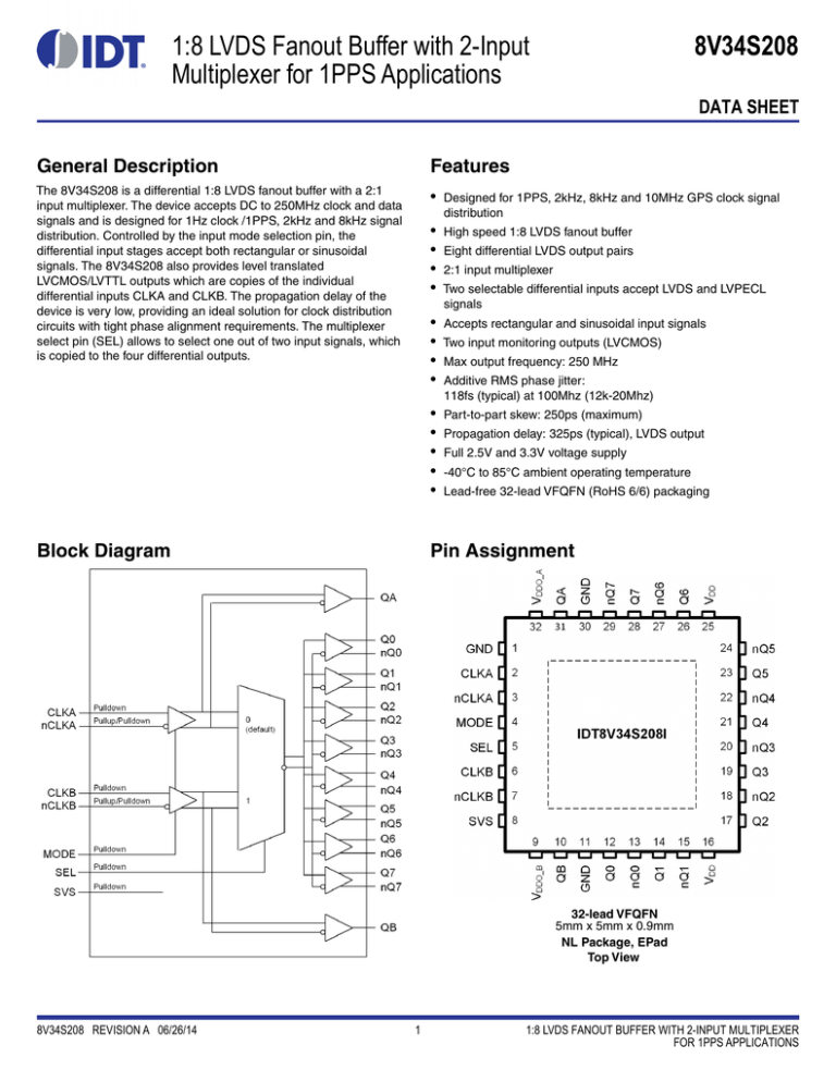
The 8V34S208 is a differential 1:8 LVDS fanout buffer with a 2:1
input multiplexer. The device accepts DC to 250MHz clock and data
signals and is designed for 1Hz clock /1PPS, 2kHz and 8kHz signal
distribution. Controlled by the input mode selection pin, the
differential input stages accept both rectangular or sinusoidal
signals. The 8V34S208 also provides level translated
LVCMOS/LVTTL outputs which are copies of the individual
differential inputs CLKA and CLKB. The propagation delay of the
device is very low, providing an ideal solution for clock distribution
circuits with tight phase alignment requirements. The multiplexer
select pin (SEL) allows to select one out of two input signals, which
is copied to the four differential outputs.
•
Designed for 1PPS, 2kHz, 8kHz and 10MHz GPS clock signal
distribution
•
•
•
•
High speed 1:8 LVDS fanout buffer
•
•
•
•
•
•
•
•
•
Block Diagram
Eight differential LVDS output pairs
2:1 input multiplexer
Two selectable differential inputs accept LVDS and LVPECL
signals
Accepts rectangular and sinusoidal input signals
Two input monitoring outputs (LVCMOS)
Max output frequency: 250 MHz
Additive RMS phase jitter:
118fs (typical) at 100Mhz (12k-20Mhz)
Part-to-part skew: 250ps (maximum)
Propagation delay: 325ps (typical), LVDS output
Full 2.5V and 3.3V voltage supply
-40°C to 85°C ambient operating temperature
Lead-free 32-lead VFQFN (RoHS 6/6) packaging
Pin Assignment
32-lead VFQFN
5mm x 5mm x 0.9mm
NL Package, EPad
Top View
8V34S208 REVISION A 06/26/14
1
1:8 LVDS FANOUT BUFFER WITH 2-INPUT MULTIPLEXER
FOR 1PPS APPLICATIONS
8V34S208 DATA SHEET
Pin Description and Pin Characteristic Tables
Table 1. Pin Descriptions
Number
Name
Type
Description
1
GND
Power
2
CLKA
Input
Pulldown
Non-inverting differential clock input.
3
nCLKA
Input
Pullup/
Pulldown
Inverting differential clock input. VDD/2 default when left floating.
4
MODE
Input
Pulldown
Input mode pin. See Table 3B. LVCMOS/LVTTL interface levels.
5
SEL
Input
Pulldown
Input selection pin. See Table 3A. LVCMOS/LVTTL interface levels.
6
CLKB
Input
Pulldown
Non-inverting differential clock input.
7
nCLKB
Input
Pullup/
Pulldown
Inverting differential clock input. VDD/2 default when left floating.
8
SVS
Input
Pulldown
Supply Voltage Select. See Table 3C. LVCMOS/LVTTL interface levels.
9
VDDO_B
Power
Output supply pin for QB output.
10
QB
Output
Single-ended QB clock output. LVCMOS/LVTTL interface levels.
11
GND
Power
Power supply ground.
12
Q0
Output
13
nQ0
Output
14
Q1
Output
15
nQ1
Output
16
VDD
Power
17
Q2
Output
18
nQ2
Output
19
Q3
Output
20
nQ3
Output
21
Q4
Output
22
nQ4
Output
23
Q5
Output
24
nQ5
Output
25
VDD
Power
26
Q6
Output
27
nQ6
Output
28
Q7
Output
29
nQ7
Output
30
GND
Power
Power supply ground.
31
QA
Output
Single-ended QA clock output. LVCMOS/LVTTL interface levels.
32
VDDO_A
Power
Output supply pin for QA output.
Power supply ground.
Differential output pair. LVDS interface levels.
Differential output pair. LVDS interface levels.
Power supply pins for the device core
Differential output pair. LVDS interface levels.
Differential output pair. LVDS interface levels.
Differential output pair. LVDS interface levels.
Differential output pair. LVDS interface levels.
Power supply pins for the device core
Differential output pair. LVDS interface levels.
Differential output pair. LVDS interface levels.
NOTE: Pullup and Pulldown refer to internal input resistors. See Table 2, Pin Characteristics, for typical values.
1:8 LVDS FANOUT BUFFER WITH 2-INPUT MULTIPLEXER
FOR 1PPS APPLICATIONS
2
REVISION A 06/26/14
8V34S208 DATA SHEET
Table 2. Pin Characteristics
Symbol
Parameter
Test Conditions
CIN
Input Capacitance
MODE, SEL, SVS
RPULLDOWN
Minimum
Typical
Maximum
Units
2
pF
Pulldown Resistor
50
k
RPULLUP
Pullup Resistor
50
k
Power Dissipation
Capacitance (per output)
VDD, VDDO_A, VDDO_B = 3.465V
6
pF
CPD
VDD, VDDO_A, VDDO_B = 2.625V
6
pF
Output
Impedance
QA, QB
VDDO_A, VDDO_B = 3.3V ± 5%
27
ROUT
QA, QB
VDDO_A, VDDO_B = 2.5V ± 5%
30
Function Tables
Table 3A. Input Selection Function Table
Input
Outputs
SEL
Q[0:7], nQ[0:7]
QA
QB
0 (default)
CLKA
CLKA
CLKB
1
CLKB
CLKA
CLKB
Table 3B. Input Mode Function Table1
Input
Operation
MODE
CLKA, CLKB
0 (default)
Inputs accept rectangular signals
1
Inputs accept sinusoidal signals
NOTE 1: Use a rectangular wave input for inputs with edge rate greater than 1V/ns.
Table 3C. Supply Voltage Select Function Table
Input
Operation
SVS
Supply Voltage
0 (default)
Set to logic 0 when VDD = VDDO_A = VDDO_B = 2.5V
1
Set to logic 1 when VDD = VDDO_A = VDDO_B = 3.3V
REVISION A 06/26/14
3
1:8 LVDS FANOUT BUFFER WITH 2-INPUT MULTIPLEXER
FOR 1PPS APPLICATIONS
8V34S208 DATA SHEET
Absolute Maximum Ratings
NOTE: Stresses beyond those listed under Absolute Maximum Ratings may cause permanent damage to the device. These ratings are stress
specifications only. Functional operation of the product at these conditions or any conditions beyond those listed in the DC Characteristics or
AC Characteristics is not implied. Exposure to absolute maximum rating conditions for extended periods may affect product reliability.
Item
Rating
Supply Voltage, VDD
4.6V
Inputs, VI
-0.5V to VDD + 0.5V
Outputs, IO (LVCMOS)
-0.5V to VDDO_X + 0.5V
Outputs, IO (LVDS)
Continuous Current
Surge Current
10mA
15mA
Maximum Junction Temperature, TJ, MAX
125°C
Storage Temperature, TSTG
-65C to 150C
ESD - Human Body Model1
ESD - Charged Device Model
2000V
1
1500V
NOTE 1: According to JEDEC/JESD 22-A114/22-C101.
DC Electrical Characteristics
Table 4A. Power Supply DC Characteristics, VDD = VDDO_A = VDDO_B = 3.3V ± 5%, TA = -40°C to 85°C
Symbol
Parameter
VDD
Test Conditions
Minimum
Typical
Maximum
Units
Power Supply Voltage
3.135
3.3
3.465
V
VDDO_A,
VDDO_B
LVCMOS Output Supply
Voltage
3.135
3.3
3.465
V
IDD
Power Supply Current
158
184
mA
IDDO_A +
IDDO_B
LVCMOS Output Supply
Current
6
8
mA
Outputs Unterminated
Table 4B. Power Supply DC Characteristics, VDD = VDDO_A = VDDO_B = 2.5V ± 5%, TA = -40°C to 85°C
Symbol
Parameter
VDD
Minimum
Typical
Maximum
Units
Power Supply Voltage
2.375
2.5
2.625
V
VDDO_A,
VDDO_B
LVCMOS Output Supply
Voltage
2.375
2.5
2.625
V
IDD
Power Supply Current
150
174
mA
IDDO_A +
IDDO_B
LVCMOS Output Supply
Current
5
8
mA
1:8 LVDS FANOUT BUFFER WITH 2-INPUT MULTIPLEXER
FOR 1PPS APPLICATIONS
Test Conditions
Outputs Unterminated
4
REVISION A 06/26/14
8V34S208 DATA SHEET
Table 4C. LVCMOS/LVTTL DC Characteristics, VDD = VDDO_A = VDDO_B = 3.3V ± 5%, TA = -40°C to 85°C
Symbol
Parameter
Test Conditions
VIH
Input High Voltage
VIL
Input Low Voltage
IIH
Input High Current
SEL, MODE, SVS
VDD = VIN = 3.465V
IIL
Input Low Current
SEL, MODE, SVS
VDD = 3.465V, VIN = 0V
-10
µA
VOH
Output High Voltage QA, QB
IOH = -8mA
2.6
V
VOL
Output Low Voltage
IOL = 8mA
QA, QB
Minimum
Typical
Maximum
Units
2.2
VDD + 0.3
V
-0.3
0.8
V
150
µA
0.5
V
Maximum
Units
Table 4D. LVCMOS/LVTTL DC Characteristics, VDD = VDDO_A = VDDO_B = 2.5V ± 5%, TA = -40°C to 85°C
Symbol
Parameter
Test Conditions
VIH
Input High Voltage
1.8
VDD + 0.3
V
VIL
Input Low Voltage
-0.3
0.6
V
IIH
Input High Current
SEL, MODE, SVS
VDD = VIN = 2.625V
150
µA
IIL
Input Low Current
SEL, MODE, SVS
VDD = 2.625V, VIN = 0V
-10
µA
VOH
Output High Voltage QA, QB
IOH = -8mA
1.8
V
VOL
Output Low Voltage
IOL = 8mA
QA, QB
Minimum
Typical
0.5
V
Table 4E. Differential DC Characteristics, VDD = 3.3V ± 5% or 2.5V ± 5%, TA = -40°C to 85°C
Symbol
Parameter
IIH
Input High Current
IIL
Input Low Current
VPP
VCMR
Peak-to-Peak
Test Conditions
CLKA, CLKB,
nCLKA, nCLKB
Typical
VDD = VIN = VDDMAX
Maximum
Units
150
µA
CLKA, CLKB
VDD = VDDMAX, VIN = 0V
-10
µA
nCLKA, nCLKB
VDD = VDDMAX, VIN = 0V
-150
µA
Voltage1
Common Mode Input
Minimum
Voltage1, 2
0.15
1.3
V
1
VDD – (VPP/2)
V
NOTE 1: VIL should not be less than -0.3V and VIH should not be higher than VDD.
NOTE 2: Common mode input voltage is defined at the crosspoint.
Table 4F. LVDS Differential DC Characteristics, VDD = 3.3V ± 5%, TA = -40°C to 85°C
Symbol
Parameter
VOD
Differential Output Voltage
VOD
VOD Magnitude Change
VOS
Offset Voltage
VOS
VOS Magnitude Change
REVISION A 06/26/14
Test Conditions
Minimum
Typical
Maximum
Units
247
390
454
mV
50
mV
1.375
V
50
mV
1.05
5
1.2
1:8 LVDS FANOUT BUFFER WITH 2-INPUT MULTIPLEXER
FOR 1PPS APPLICATIONS
8V34S208 DATA SHEET
Table 4G. LVDS Differential DC Characteristics, VDD = 2.5V ± 5%, TA = -40°C to 85°C
Symbol
Parameter
Test Conditions
VOD
Differential Output Voltage
VOD
VOD Magnitude Change
VOS
Offset Voltage
VOS
VOS Magnitude Change
Minimum
Typical
Maximum
Units
247
373
454
mV
50
mV
1.375
V
50
mV
Maximum
Units
250
MHz
1.05
1.2
AC Electrical Characteristics
Table 5. AC Characteristics, VDD = VDDO_A = VDDO_B = 3.3V ±5% or 2.5V ±5%, TA = -40°C to 85°C1
Symbol
Parameter
fOUT
Output Frequency
V/t
Test Conditions
2
CLKA, CLKB
Propagation Delay3
CLKA, CLKB to
Q[0-3], nQ[0-3]
200
325
434
ps
Propagation Delay4
CLKA, CLKB to
QA, QB
970
1.20
1.62
ns
118
170
fs
tjit(Ø)
Buffer Additive
Phase Jitter, RMS;
Refer to Additive
Phase Jitter Section
tsk(pp)
Part-to-Part Skew5 6 Q[0-3], nQ[0-3]
tsk(o)
Typical
Input Edge Rate
tPD
Output
Skew6
Q[0-3], nQ[0-3]
MODE = 0
Minimum
1
fOUT = 156.25MHz,
Integration Range:
12kHz – 20MHz,
MODE 0
V/ns
250
ps
Q[0-3], nQ[0-3]7
65
ps
8
65
ps
1.3
ns
QA-QB
All outputs
tsk(p)
Pulse Skew9, 10
tR / tF
Output Rise/
Fall Time
MUXISOLATION
MUX Isolation11
Q[0-3], nQ[0-3]
11
62
ps
QA, QB
75
140
ps
QA, QB;
20% to 80%
200
350
ps
Q[0-3], nQ[0-3]
20% to 80%
125
250
ps
fOUT = 100.00MHz,
VPP = 400mV
53
dB
NOTE 1: Electrical parameters are guaranteed over the specified ambient operating temperature range, which is established when the device
is mounted in a test socket with maintained transverse airflow greater than 500 lfpm. The device will meet specifications after thermal
equilibrium has been reached under these conditions.
NOTE 2: In MODE = 1 sinusoidal input signals are permitted and no minimum input edge rate specification applies.
NOTE 3: Measured from the differential input crosspoint to the differential output crosspoint using an input with 50% duty cycle.
NOTE 4: Measured from the differential input crosspoint to the output at VDDO_X/2 using an input with 50% duty cycle.
NOTE 5: Defined as skew between outputs on different devices operating at the same supply voltage, same frequency, same temperature and
with equal load conditions. Using the same type of inputs on each device, the outputs are measured at the differential crosspoints.
NOTE 6: This parameter is defined in accordance with JEDEC Standard 65.
NOTE 7: Defined as skew between outputs at the same supply voltage and with equal load conditions. Measured at the differential crosspoints.
NOTE 8: Defined as skew between outputs at the same supply voltage and with equal load conditions. Measured at VDDO_X/2 of the output.
NOTE 9: Output pulse skew tSK(P) is the absolute difference of the propagation delay times: | tPLH – tPHL |.
NOTE 10: odc = input duty cycle ± (tSK(p)/2 * 1/Output Period) * 100
NOTE 11: Qx, nQx output measured differentially. See Parameter Measurement Information for MUX Isolation diagram.
1:8 LVDS FANOUT BUFFER WITH 2-INPUT MULTIPLEXER
FOR 1PPS APPLICATIONS
6
REVISION A 06/26/14
8V34S208 DATA SHEET
Table 6. Characteristics for 1PPS operation, VDD = 3.3V ±5% or VDD = 2.5V ±5%, TA = -40°C to 85°C1 2 3 4
Symbol
Parameter
T
Input and Output Pulse Period
TP
Positive or Negative Pulse Width
tPD
Propagation Delay;
CLKx/nCLKx to Qx/nQx
300
650
ps
tsk(p)
Pulse Width Distortion
CLKx/nCLKx to Qx/nQx
55
300
ps
325
ps
350
ps
350
ps
tsk(o)
Test Conditions
5
Output Skew
Minimum
Typical
1
Part-to-Part
tR / tF
Output Rise/Fall Time
ns
Qx/nQx to Qy/nQy
10% to 90%
50
Units
s
100
Skew6
tsk(pp)
Maximum
150
NOTE 1: 1PPS (one pulse per second) signals are defined as repetitive pulses with a rate (period) of 1Hz. The positive input pulse width may
vary. The active signal edge is the rising edge. Parameters in this table are characterized for a positive input pulse width of 100ns,
100ms and 500ms; All device interfaces are DC-coupled. Parameters are defined in accordance with ITU-T G.703 Amendment 1 Specifications for the physical layer of the ITU-T G8271/Y.1366 time synchronization interfaces.
NOTE 2: Electrical parameters are guaranteed over the specified ambient operating temperature range, which is established when the device
is mounted in a test socket with maintained transverse airflow greater than 500lfpm. The device will meet specifications after thermal
equilibrium has been reached under these conditions.
NOTE 3: tPD, tSK(O), tSK(P) and tSK(P) parameters of differential signals are referenced to the crosspoint.
NOTE 4: Differential outputs for 1PPS signal transmission are terminated balanced 100 according to the LVDS Output Load Test Circuit
figures. The dedicated 1PPS outputs are the differential outputs Q0-Q3.
NOTE 5: This parameter is defined in accordance with JEDEC Standard 65.
NOTE 6: Defined as skew between outputs on different devices operating at the same supply voltages and with equal load conditions. Each
device uses the same type of input.
REVISION A 06/26/14
7
1:8 LVDS FANOUT BUFFER WITH 2-INPUT MULTIPLEXER
FOR 1PPS APPLICATIONS
8V34S208 DATA SHEET
Additive Phase Jitter
of the power in the 1Hz band to the power in the fundamental. When
the required offset is specified, the phase noise is called a dBc value,
which simply means dBm at a specified offset from the fundamental.
By investigating jitter in the frequency domain, we get a better
understanding of its effects on the desired application over the entire
time record of the signal. It is mathematically possible to calculate an
expected bit error rate given a phase noise plot.
SSB Phase Noise (dBc/Hz)
The spectral purity in a band at a specific offset from the fundamental
compared to the power of the fundamental is called the dBc Phase
Noise. This value is normally expressed using a Phase noise plot
and is most often the specified plot in many applications. Phase noise
is defined as the ratio of the noise power present in a 1Hz band at a
specified offset from the fundamental frequency to the power value of
the fundamental. This ratio is expressed in decibels (dBm) or a ratio
Offset from Carrier Frequency (Hz)
Measured using an Rohde & Schwarz SMA100 as the input source.
As with most timing specifications, phase noise measurements have
issues relating to the limitations of the equipment. Often the noise
floor of the equipment is higher than the noise floor of the device. This
is illustrated above. The device meets the noise floor of what is
shown, but can actually be lower. The phase noise is dependent on
the input source and measurement equipment.
1:8 LVDS FANOUT BUFFER WITH 2-INPUT MULTIPLEXER
FOR 1PPS APPLICATIONS
8
REVISION A 06/26/14
8V34S208 DATA SHEET
Parameter Measurement Information
VDD
VDD
GND
2.5V LVDS Output Load Test Circuit
3.3V LVDS Output Load Test Circuit
1.25V±5%
1.65V±5%
SCOPE
VDD
VDDO_A
VDDO_B
SCOPE
VDD
VDDO_A
VDDO_B
Qx
GND
Qx
GND
-1.25±5%
-1.65V±5%
2.5V Core/2.5V LVCMOS Output Load Test Circuit
3.3V Core/3.3V LVCMOS Output Load Test Circuit
VDD
Par t 1
nQx
nCLK[A:B]
Qx
V
PP
Cross Points
nQx
CLK[A:B]
Par t 2
V
CMR
Qx
tsk(pp)
GND
Differential Input Level
REVISION A 06/26/14
Part-to-Part Skew
9
1:8 LVDS FANOUT BUFFER WITH 2-INPUT MULTIPLEXER
FOR 1PPS APPLICATIONS
8V34S208 DATA SHEET
Parameter Measurement Information, Continued
nQx
V
DDO_X
Qx
Qx
2
nQy
V
DDO_X
Qy
Qy
LVDS Output Skew
2
tsk(o)
LVCMOS Output Skew
nCLK[A:B]
nCLK[A:B]
CLK[A:B]
CLK[A:B]
nQx
VDDO_X
2
t
Q[A:B]
Qx
tPD
PD
Differential Propagation Delay
Propagation Delay
nQ[0:7]
80%
80%
80%
80%
VOD
20%
20%
Q[A:B]
tR
LVCMOS Output Rise/Fall Time
1:8 LVDS FANOUT BUFFER WITH 2-INPUT MULTIPLEXER
FOR 1PPS APPLICATIONS
20%
20%
Q[0:7]
tF
tR
tF
LVDS Output Rise/Fall Time
10
REVISION A 06/26/14
8V34S208 DATA SHEET
Parameter Measurement Information, Continued
nCLK[A:B]
nCLK[A:B]
CLK[A:B]
CLK[A:B]
nQx
V
DDO_X
V
DDO_X
Qx
Q[A:B]
t PLH
t PHL
t PLH
tsk(p)= |t PHL - t PLH|
2
2
t PHL
tsk(p)= |t PHL - t PLH|
Differential Pulse Skew
Pulse Skew
Differential Output Voltage Setup
Offset Voltage Setup
Spectrum of Output Signal Q
MUX selects active
input clock signal
Amplitude (dB)
A0
MUX_ISOLATION = A0 – A1
MUX selects other input
A1
(fundamental)
Frequency
MUX Isolation
REVISION A 06/26/14
11
1:8 LVDS FANOUT BUFFER WITH 2-INPUT MULTIPLEXER
FOR 1PPS APPLICATIONS
8V34S208 DATA SHEET
Applications Information
Wiring the Differential Input to Accept Single-Ended Levels
impedance. For most 50 applications, R3 and R4 can be 100. The
values of the resistors can be increased to reduce the loading for
slower and weaker LVCMOS driver. When using single-ended
signaling, the noise rejection benefits of differential signaling are
reduced. Even though the differential input can handle full rail
LVCMOS signaling, it is recommended that the amplitude be
reduced. The datasheet specifies a lower differential amplitude,
however this only applies to differential signals. For single-ended
applications, the swing can be larger, however VIL cannot be less
than -0.3V and VIH cannot be more than VDD + 0.3V. Though some
of the recommended components might not be used, the pads
should be placed in the layout. They can be utilized for debugging
purposes. The datasheet specifications are characterized and
guaranteed by using a differential signal.
Figure 1 shows how a differential input can be wired to accept single
ended levels. The reference voltage V1= VDD/2 is generated by the
bias resistors R1 and R2. The bypass capacitor (C1) is used to help
filter noise on the DC bias. This bias circuit should be located as close
to the input pin as possible. The ratio of R1 and R2 might need to be
adjusted to position the V1in the center of the input voltage swing. For
example, if the input clock swing is 2.5V and VDD = 3.3V, R1 and R2
value should be adjusted to set V1 at 1.25V. The values below are for
when both the single ended swing and VDD are at the same voltage.
This configuration requires that the sum of the output impedance of
the driver (Ro) and the series resistance (Rs) equals the transmission
line impedance. In addition, matched termination at the input will
attenuate the signal in half. This can be done in one of two ways.
First, R3 and R4 in parallel should equal the transmission line
Figure 1. Recommended Schematic for Wiring a Differential Input to Accept Single-ended Levels
1:8 LVDS FANOUT BUFFER WITH 2-INPUT MULTIPLEXER
FOR 1PPS APPLICATIONS
12
REVISION A 06/26/14
8V34S208 DATA SHEET
3.3V Differential Clock Input Interface
common driver types. The input interfaces suggested here are
examples only. If the driver is from another vendor, use their
termination recommendation. Please consult with the vendor of the
driver component to confirm the driver termination requirements.
The CLK /nCLK accepts LVDS, LVPECL and other differential
signals. Both differential signals must meet the VPP and VCMR input
requirements. Figure 2A to Figure 2C show interface examples for
the CLK/nCLK input with built-in 50 terminations driven by the most
3.3V
3.3V
3.3V
3.3V
3.3V
Zo = 50Ω
CLK
CLK
Zo = 50Ω
nCLK
LVPECL
nCLK
R1
50Ω
Differential
Input
LVPECL
R2
50Ω
Differential
Input
R2
50Ω
Figure 2A. CLK/nCLK Input Driven by a
3.3V LVPECL Driver
Figure 2C. CLK/nCLK Input Driven by a
3.3V LVPECL Driver
3.3V
3.3V
Zo = 50Ω
CLK
R1
100Ω
Zo = 50Ω
LVDS
nCLK
Receiver
Figure 2B. CLK/nCLK Input Driven by a
3.3V LVDS Driver
REVISION A 06/26/14
13
1:8 LVDS FANOUT BUFFER WITH 2-INPUT MULTIPLEXER
FOR 1PPS APPLICATIONS
8V34S208 DATA SHEET
2.5V Differential Clock Input Interface
common driver types. The input interfaces suggested here are
examples only. If the driver is from another vendor, use their
termination recommendation. Please consult with the vendor of the
driver component to confirm the driver termination requirements.
The CLK /nCLK accepts LVDS, LVPECL and other differential
signals. Both differential signals must meet the VPP and VCMR input
requirements. Figure 3A to Figure 3C show interface examples for
the CLK/nCLK input with built-in 50 terminations driven by the most
2.5V
2.5V
2.5V
2.5V
2.5V
R3
250
Zo = 50
CLK
R4
250
Zo = 50
CLK
Zo = 50
nCLK
R1
50
Zo = 50
Differential
Input
LVPECL
R2
50
nCLK
LVPECL
R1
62.5
R2
62.5
Differential
Input
R3
18
Figure 3A. CLK/nCLK Input Driven by a
2.5V LVPECL Driver
Figure 3C. CLK/nCLK Input Driven by a
2.5V LVPECL Driver
2.5V
2.5V
Zo = 50
CLK
R1
100
Zo = 50
LVDS
nCLK
Differential
Input
Figure 3B. CLK/nCLK Input Driven by a
2.5V LVDS Driver
1:8 LVDS FANOUT BUFFER WITH 2-INPUT MULTIPLEXER
FOR 1PPS APPLICATIONS
14
REVISION A 06/26/14
8V34S208 DATA SHEET
Recommendations for Unused Input and Output Pins
Inputs:
Outputs:
LVCMOS Control Pins
LVDS Outputs
All control pins have internal pulldown resistors; additional resistance
is not required but can be added for additional protection. A 1k
resistor can be used.
All unused LVDS output pairs can be either left floating or terminated
with 100 across. If they are left floating there should be no trace
attached.
CLK/nCLK Input
For applications not requiring the use of the differential input, both
CLK and nCLK can be left floating. Though not required, but for
additional protection, a 1k resistor can be tied from CLK to ground.
REVISION A 06/26/14
15
1:8 LVDS FANOUT BUFFER WITH 2-INPUT MULTIPLEXER
FOR 1PPS APPLICATIONS
8V34S208 DATA SHEET
LVDS Driver Termination
with either type of output structure. Figure 4B, which can also be
used with both output types, is an optional termination with center tap
capacitance to help filter common mode noise. The capacitor value
should be approximately 50pF. If using a non-standard termination, it
is recommended to contact IDT and confirm if the output structure is
current source or voltage source type. In addition, since these
outputs are LVDS compatible, the input receiver’s amplitude and
common-mode input range should be verified for compatibility with
the output.
For a general LVDS interface, the recommended value for the
termination impedance (ZT) is between 90 and 132. The actual
value should be selected to match the differential impedance (Z0) of
your transmission line. A typical point-to-point LVDS design uses a
100 parallel resistor at the receiver and a 100 differential
transmission-line environment. In order to avoid any
transmission-line reflection issues, the components should be
surface mounted and must be placed as close to the receiver as
possible. IDT offers a full line of LVDS compliant devices with two
types of output structures: current source and voltage source. The
standard termination schematic as shown in Figure 4A can be used
LVDS
Driver
ZO ZT
LVDS
Receiver
ZT
Figure 4A. Standard Termination
LVDS
Driver
ZT
2
ZO ZT
C
ZT
2
LVDS
Receiver
Figure 4B. Optional Termination
1:8 LVDS FANOUT BUFFER WITH 2-INPUT MULTIPLEXER
FOR 1PPS APPLICATIONS
16
REVISION A 06/26/14
8V34S208 DATA SHEET
Power Considerations – LVDS Outputs
This section provides information on power dissipation and junction temperature for the 8V34S208. Equations and example calculations are
also provided.
1.
Power Dissipation.
The total power dissipation for the 8V34S208 is the sum of the core power plus the analog power plus the power dissipated in the load(s). The
following is the power dissipation for VDD = 3.3V + 5% = 3.465V, which gives worst case results.
The maximum current at 85°C is as follows:
IDD = 184mA
IDDOA = 4mA
IDDOB = 4mA
•
Power (core, LVDS)MAX = VDD_MAX * (IDD_MAX + IDDOA_MAX + IDDOB_MAX)
= 3.465V * (184mA + 4mA + 4mA) = 665.28mW
LVCMOS Output Power Dissipation
•
Dynamic Power Dissipation at 200MHz
Power (250MHz) = CPD * Frequency * (VDDOX_MAX)2 = 6pF * 250MHz * (3.465V)2 = 18.01mW per output
Total CMOS Power = 2 * 18.01mW = 36.02mW
Total Power_MAX = 665.28mW + 36.02mW = 701.3mW
2. Junction Temperature.
Junction temperature, Tj, is the temperature at the junction of the bond wire and bond pad directly affects the reliability of the device. The
maximum recommended junction temperature is 125°C. Limiting the internal transistor junction temperature, Tj, to 125°C ensures that the bond
wire and bond pad temperature remains below 125°C.
The equation for Tj is as follows: Tj = JA * Pd_total + TA
Tj = Junction Temperature
JA = Junction-to-Ambient Thermal Resistance
Pd_total = Total Device Power Dissipation (example calculation is in section 1 above)
TA = Ambient Temperature
In order to calculate junction temperature, the appropriate junction-to-ambient thermal resistance JA must be used. Assuming no air flow and
a multi-layer board, the appropriate value is 48.9°C/W per Table 7 below.
Therefore, Tj for an ambient temperature of 85°C with all outputs switching is:
85°C + 0.701W * 48.9°C/W = 119.29°C. This is below the limit of 125°C.
This calculation is only an example. Tj will obviously vary depending on the number of loaded outputs, supply voltage, air flow and the type of
board (multi-layer).
Table 7. Thermal Resistance JA for 32-Lead VFQFN
JA vs. Air Flow
Meters per Second
Multi-Layer PCB, JEDEC Standard Test Boards
REVISION A 06/26/14
0
1
2
48.9°C/W
42.0°C/W
39.4°C/W
17
1:8 LVDS FANOUT BUFFER WITH 2-INPUT MULTIPLEXER
FOR 1PPS APPLICATIONS
8V34S208 DATA SHEET
Reliability Information
Table 8. JA vs. Air Flow Table for a 32-Lead VFQFN
JA vs. Air Flow
Meters per Second
Multi-Layer PCB, JEDEC Standard Test Boards
0
1
2
48.9°C/W
42.0°C/W
39.4°C/W
Transistor Count
The transistor count for the 8V34S208 is: 492
1:8 LVDS FANOUT BUFFER WITH 2-INPUT MULTIPLEXER
FOR 1PPS APPLICATIONS
18
REVISION A 06/26/14
8V34S208 DATA SHEET
32-Lead VFQFN Package Outline and Package Dimensions
REVISION A 06/26/14
19
1:8 LVDS FANOUT BUFFER WITH 2-INPUT MULTIPLEXER
FOR 1PPS APPLICATIONS
8V34S208 DATA SHEET
Ordering Information
Table 9. Ordering Information
Part/Order Number
8V34S208NLGI
8V34S208NLGI8
Marking
IDT8V34S208NLGI
IDT8V34S208NLGI
1:8 LVDS FANOUT BUFFER WITH 2-INPUT MULTIPLEXER
FOR 1PPS APPLICATIONS
Package
“Lead-Free” 32-Lead VFQFN
“Lead-Free” 32-Lead VFQFN
20
Shipping Packaging
Tray
Tape & Reel
Temperature
-40C to 85C
-40C to 85C
REVISION A 06/26/14
Corporate Headquarters
Sales
Tech Support
6024 Silver Creek Valley Road
San Jose, CA 95138 USA
1-800-345-7015 or 408-284-8200
Fax: 408-284-2775
www.IDT.com
email: clocks@idt.com
DISCLAIMER Integrated Device Technology, Inc. (IDT) and its subsidiaries reserve the right to modify the products and/or specifications described herein at any time and at IDT’s sole discretion. All information in
this document, including descriptions of product features and performance, is subject to change without notice. Performance specifications and the operating parameters of the described products are determined
in the independent state and are not guaranteed to perform the same way when installed in customer products. The information contained herein is provided without representation or warranty of any kind, whether
express or implied, including, but not limited to, the suitability of IDT’s products for any particular purpose, an implied warranty of merchantability, or non-infringement of the intellectual property rights of others. This
document is presented only as a guide and does not convey any license under intellectual property rights of IDT or any third parties.
IDT’s products are not intended for use in applications involving extreme environmental conditions or in life support systems or similar devices where the failure or malfunction of an IDT product can be reasonably
expected to significantly affect the health or safety of users. Anyone using an IDT product in such a manner does so at their own risk, absent an express, written agreement by IDT.
While the information presented herein has been checked for both accuracy and reliability, Integrated Device Technology (IDT) assumes no responsibility for either its use or for the infringement of any patents or
other rights of third parties, which would result from its use. No other circuits, patents, or licenses are implied. This product is intended for use in normal commercial applications. Any other applications, such as
those requiring extended temperature ranges, high reliability or other extraordinary environmental requirements are not recommended without additional processing by IDT. IDT reserves the right to change any
circuitry or specifications without notice. IDT does not authorize or warrant any IDT product for use in life support devices or critical medical instruments.
Integrated Device Technology, IDT and the IDT logo are registered trademarks of IDT. Product specification subject to change without notice. Other trademarks and service marks used herein, including protected
names, logos and designs, are the property of IDT or their respective third party owners.
Copyright ©2014 Integrated Device Technology, Inc.. All rights reserved.
