Clock Distribution Fanout Buffers
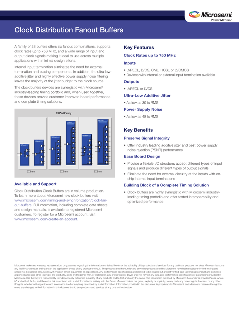
A family of 28 buffers offers six fanout combinations, supports
clock rates up to 750 MHz, and a wide range of input and
output clock signals making it ideal to use across multiple
applications with minimal design efforts.
Internal input termination eliminates the need for external
termination and biasing components. In addition, the ultra lowadditive jitter and highly effective power supply noise filtering
leaves the majority of the jitter budget to the clock source.
The clock buffers devices are synergistic with Microsemi®
industry-leading timing portfolio and, when used together,
these devices provide customer improved board performance
and complete timing solutions.
Key Features
Clock Rates up to 750 MHz
Inputs
• LVPECL, LVDS, CML, HCSL or LVCMOS
• Devices with internal or external input termination available
Outputs
• LVPECL or LVDS
Ultra-Low Additive Jitter
• As low as 39 fs RMS
Power Supply Noise
28 Part Family
• As low as 48 fs RMS
2:8 Fanout
1:8 Fanout
Key Benefits
2:6 Fanout
Preserve Signal Integrity
1:6 Fanout
1:4 Fanout
• Offer industry leading additive jitter and best power supply
noise rejection (PSNR) performance
1:2 Fanout
Ease Board Design
3X3mm
5X5mm
5X5mm
• Provide a flexible I/O structure; accept different types of input
signals and produce different types of output signals
• Eliminate the need for external circuitry at the inputs with onchip internal input terminations
Available and Support
Building Block of a Complete Timing Solution
Clock Distribution Clock Buffers are in volume production.
To learn more about Microsemi new clock buffers visit
www.microsemi.com/timing-and-synchronization/clock-fanout-buffers. Full information, including complete data sheets
and design manuals, is available to registered Microsemi
customers. To register for a Microsemi account, visit
www.microsemi.com/create-an-account.
• Clock buffers are highly synergistic with Microsemi industryleading timing portfolio and offer tested interoperability and
optimized performance
Microsemi makes no warranty, representation, or guarantee regarding the information contained herein or the suitability of its products and services for any particular purpose, nor does Microsemi assume
any liability whatsoever arising out of the application or use of any product or circuit. The products sold hereunder and any other products sold by Microsemi have been subject to limited testing and
should not be used in conjunction with mission-critical equipment or applications. Any performance specifications are believed to be reliable but are not verified, and Buyer must conduct and complete
all performance and other testing of the products, alone and together with, or installed in, any end-products. Buyer shall not rely on any data and performance specifications or parameters provided by
Microsemi. It is the Buyer’s responsibility to independently determine suitability of any products and to test and verify the same. The information provided by Microsemi hereunder is provided “as is, where
is” and with all faults, and the entire risk associated with such information is entirely with the Buyer. Microsemi does not grant, explicitly or implicitly, to any party any patent rights, licenses, or any other
IP rights, whether with regard to such information itself or anything described by such information. Information provided in this document is proprietary to Microsemi, and Microsemi reserves the right to
make any changes to the information in this document or to any products and services at any time without notice.
Clock Distribution Fanout Buffers
Preserve Signal Integrity, Ease Board Design With Microsemi Clock Distribution Fanout Buffers
Today’s modern systems often require the distribution of several
clock frequencies to multiple loads. Clock buffers complement
clock synthesis devices by providing additional fanout capability
as needed.
The ability to create multiple copies of a clock signal and
distribute them among several loads with minimal additive jitter
is a key advantage of a strong clock management solution.
Jitter budget is mostly dedicated to the clock source and very
little is left for clock management. Microsemi high performance
buffers add minimal jitter combined with industry leading power
supply noise filtering. This results in reduced system cost and
easier design.
Output
Input
Type
Termination
1:4
Buffers with internal termination reduce the need for external
components to save board cost and complexity. Buffers
without internal termination support the use of precision
external termination components and additional termination
methods.
The family offers six fanout combinations—1:2, 1:4, 1:6,
1:8, 2:6, and 2:8—all available with internal or external input
termination and LVDS or LVPECL outputs. These options
provide the ideal devices for meeting application needs and
easing component sourcing requirements.
This family of buffers has a flexible I/O structure where inputs
1:2
are compatible with LVPECL, LVDS, CML, HCSL, LVCMOS,
HSTL and SSTL, and outputs support LVPECL and LVDS
signals.
1:6
1:8
2:6
2:8
Glitch-Free Switching
2:8
Simple Switching
QFN-16
3x3mm
QFN-16
3x3mm
QFN-32
5x5mm
QFN-32
5x5mm
QFN-32
5x5mm
QFN-32
5x5mm
QFN-32
5x5mm
External
ZL40200
ZL40202
ZL40204
ZL40206
ZL40208
ZL40210
ZL40224
Internal
ZL40201
ZL40203
ZL40205
ZL40207
ZL40209
ZL40211
ZL40225
External
ZL40212
ZL40214
ZL40216
ZL40218
ZL40220
ZL40222
ZL40226
Internal
ZL40213
ZL40215
ZL40217
ZL40219
ZL40221
ZL40223
ZL40227
LVPECL
LVDS
Microsemi Corporate Headquarters
One Enterprise, Aliso Viejo, CA 92656 USA
Within the USA: +1 (800) 713-4113
Outside the USA: +1 (949) 380-6100
Sales: +1 (949) 380-6136
Fax: +1 (949) 215-4996
email: sales.support@microsemi.com
www.microsemi.com
Microsemi Corporation (Nasdaq: MSCC) offers a comprehensive portfolio of semiconductor and system solutions
for communications, defense & security, aerospace and industrial markets. Products include high-performance and
radiation-hardened analog mixed-signal integrated circuits, FPGAs, SoCs and ASICs; power management products;
timing and synchronization devices and precise time solutions, setting the world’s standard for time; voice processing
devices; RF solutions; discrete components; security technologies and scalable anti-tamper products; Power-overEthernet ICs and midspans; as well as custom design capabilities and services. Microsemi is headquartered in Aliso
Viejo, Calif., and has approximately 3,400 employees globally. Learn more at www.microsemi.com.
©2015 Microsemi Corporation. All rights reserved. Microsemi and the Microsemi logo are registered trademarks of Microsemi Corporation. All other
trademarks and service marks are the property of their respective owners.
CDFB-3-15
