MAX14934–MAX14936 Four-Channel, 5kVRMS Digital Isolators
advertisement
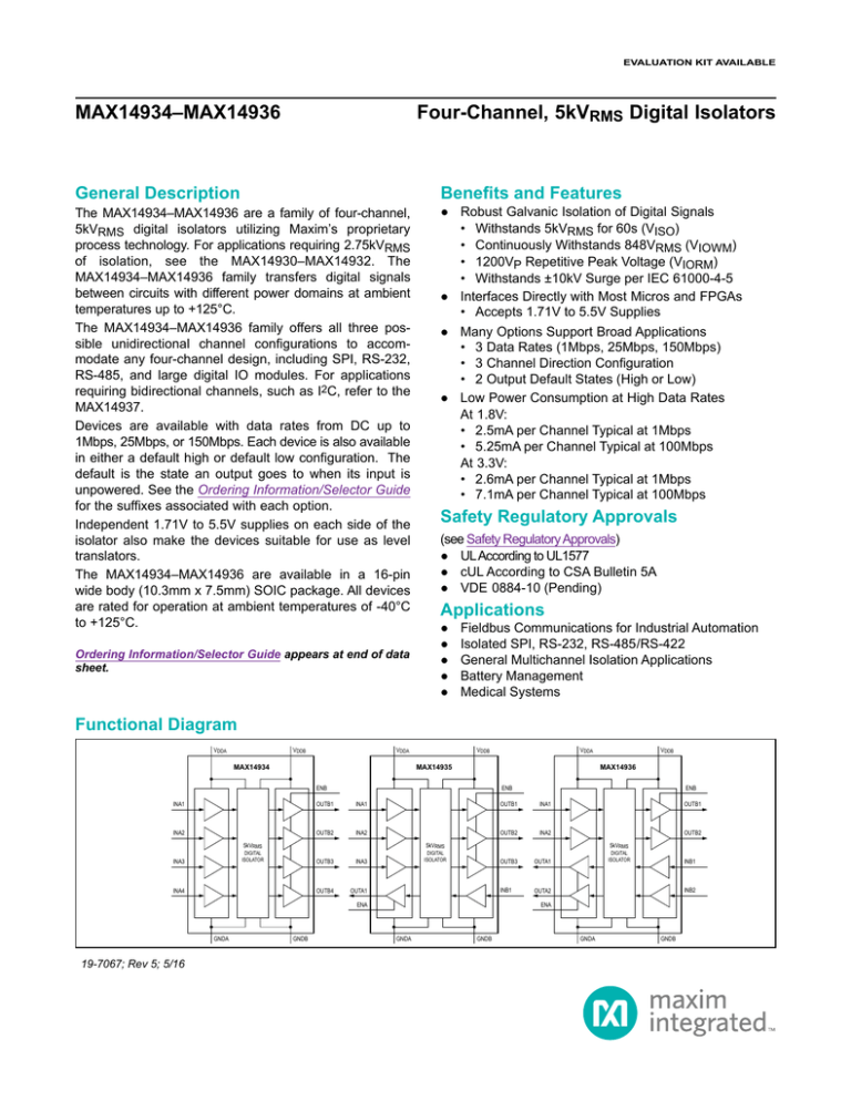
EVALUATION KIT AVAILABLE MAX14934–MAX14936 Four-Channel, 5kVRMS Digital Isolators General Description The MAX14934–MAX14936 are a family of four-channel, 5kVRMS digital isolators utilizing Maxim’s proprietary process technology. For applications requiring 2.75kVRMS of isolation, see the MAX14930–MAX14932. The MAX14934–MAX14936 family transfers digital signals between circuits with different power domains at ambient temperatures up to +125°C. The MAX14934–MAX14936 family offers all three possible unidirectional channel configurations to accommodate any four-channel design, including SPI, RS-232, RS-485, and large digital IO modules. For applications requiring bidirectional channels, such as I2C, refer to the MAX14937. Devices are available with data rates from DC up to 1Mbps, 25Mbps, or 150Mbps. Each device is also available in either a default high or default low configuration. The default is the state an output goes to when its input is unpowered. See the Ordering Information/Selector Guide for the suffixes associated with each option. Independent 1.71V to 5.5V supplies on each side of the isolator also make the devices suitable for use as level translators. The MAX14934–MAX14936 are available in a 16-pin wide body (10.3mm x 7.5mm) SOIC package. All devices are rated for operation at ambient temperatures of -40°C to +125°C. Ordering Information/Selector Guide appears at end of data sheet. Benefits and Features ● Robust Galvanic Isolation of Digital Signals • Withstands 5kVRMS for 60s (VISO) • Continuously Withstands 848VRMS (VIOWM) • 1200VP Repetitive Peak Voltage (VIORM) • Withstands ±10kV Surge per IEC 61000-4-5 ● Interfaces Directly with Most Micros and FPGAs • Accepts 1.71V to 5.5V Supplies ● Many Options Support Broad Applications • 3 Data Rates (1Mbps, 25Mbps, 150Mbps) • 3 Channel Direction Configuration • 2 Output Default States (High or Low) ● Low Power Consumption at High Data Rates At 1.8V: • 2.5mA per Channel Typical at 1Mbps • 5.25mA per Channel Typical at 100Mbps At 3.3V: • 2.6mA per Channel Typical at 1Mbps • 7.1mA per Channel Typical at 100Mbps Safety Regulatory Approvals (see Safety Regulatory Approvals) ● UL According to UL1577 ● cUL According to CSA Bulletin 5A ● VDE 0884-10 (Pending) Applications ● ● ● ● ● Fieldbus Communications for Industrial Automation Isolated SPI, RS-232, RS-485/RS-422 General Multichannel Isolation Applications Battery Management Medical Systems Functional Diagram VDDA VDDA VDDB MAX14934 INA2 ENB OUTB1 INA1 OUTB2 INA2 INA4 19-7067; Rev 5; 5/16 INA1 OUTB2 INA2 OUTB1 OUTB2 OUTB3 INA3 OUTB4 OUTA1 5kVRMS DIGITAL ISOLATOR ENA GNDA ENB OUTB1 5kVRMS 5kVRMS DIGITAL ISOLATOR GNDB VDDB MAX14936 ENB INA1 INA3 VDDA VDDB MAX14935 OUTB3 OUTA1 INB1 OUTA2 DIGITAL ISOLATOR INB1 INB2 ENA GNDA GNDB GNDA GNDB MAX14934–MAX14936 Four-Channel, 5kVRMS Digital Isolators Absolute Maximum Ratings VDDA to GNDA, VDDB to GNDB..............................-0.3V to +6V INA_, ENA to GNDA.................................................-0.3V to +6V INB_, ENB to GNDB................................................-0.3V to +6V OUTA_ to GNDA..................................... -0.3V to (VDDA + 0.3V) OUTB_ to GNDB..................................... -0.3V to (VDDB + 0.3V) Short-Circuit Duration (OUTA_ to GNDA, OUTB_ to GNDB) ...................Continuous Continuous Power Dissipation (TA = +70°C) Wide SOIC (derate 14.1mW/°C above +70°C)....... 1126.8mW Operating Temperature Range.......................... -40°C to +125°C Maximum Junction Temperature......................................+150°C Storage Temperature Range............................. -65°C to +150°C Lead Temperature (soldering, 10s).................................. +300°C Soldering Temperature (reflow) .......................................+260°C Stresses beyond those listed under “Absolute Maximum Ratings” may cause permanent damage to the device. These are stress ratings only, and functional operation of the device at these or any other conditions beyond those indicated in the operational sections of the specifications is not implied. Exposure to absolute maximum rating conditions for extended periods may affect device reliability. Package Thermal Characteristics (Note 1) Wide SOIC Junction-to-Ambient Thermal Resistance (θJA)...........71°C/W Junction-to-Case Thermal Resistance (θJC)................23°C/W Note 1: Package thermal resistances were obtained using the method described in JEDEC specification JESD51-7, using a four-layer board. For detailed information on package thermal considerations, refer to www.maximintegrated.com/thermal-tutorial. DC Electrical Characteristics (VDDA - VGNDA = +1.71V to +5.5V, VDDB - VGNDB = +1.71V to +5.5V, CL = 15pF, TA = -40°C to +125°C, unless otherwise noted. Typical values are at VDDA - VGNDA = +3.3V, VDDB - VGNDB = +3.3V, VGNDA = VGNDB, TA = +25°C, unless otherwise noted.) (Note 2) PARAMETER SYMBOL CONDITIONS MIN TYP MAX UNITS 5.5 V 5.5 V 1.71 V POWER SUPPLY Operating Supply Voltage VDDA Relative to GNDA 1.71 VDDB Relative to GNDB 1.71 VDD_ rising 1.45 Undervoltage Lockout Threshold VUVLO_ Undervoltage Lockout Threshold Hysteresis VUVLO_ www.maximintegrated.com HYST 1.58 50 mV Maxim Integrated │ 2 MAX14934–MAX14936 Four-Channel, 5kVRMS Digital Isolators DC Electrical Characteristics (continued) (VDDA - VGNDA = +1.71V to +5.5V, VDDB - VGNDB = +1.71V to +5.5V, CL = 15pF, TA = -40°C to +125°C, unless otherwise noted. Typical values are at VDDA - VGNDA = +3.3V, VDDB - VGNDB = +3.3V, VGNDA = VGNDB, TA = +25°C, unless otherwise noted.) (Note 2) PARAMETER SYMBOL CONDITIONS 500kHz square wave IDDA 12.5MHz square wave (Note 3) 50MHz square wave (Note 3) Supply Current (MAX14934_) 500kHz square wave IDDB 12.5MHz square wave (Note 3) 50MHz square wave (Note 3) www.maximintegrated.com MIN TYP MAX VDDA = 5V 1.2 1.9 VDDA = 3.3V 1.2 1.9 VDDA = 2.5V 1.2 1.9 VDDA = 1.8V 1.1 1.9 VDDA = 5V 2.1 2.7 VDDA = 3.3V 2 2.7 VDDA = 2.5V 2 2.7 VDDA = 1.8V 2 2.6 VDDA = 5V 5 6.6 VDDA = 3.3V 4.6 6.1 VDDA = 2.5V 4.5 6.0 VDDA = 1.8V 4.5 6.0 VDDB = 5V 8.1 11.2 VDDB = 3.3V 7.9 11.1 VDDB = 2.5V 7.9 11.0 VDDB = 1.8V 7.7 10.8 VDDB = 5V 12.8 15.9 VDDB = 3.3V 11.1 14.2 VDDB = 2.5V 10.2 13.4 VDDB = 1.8V 9.4 12.4 VDDB = 5V 27.2 35.4 VDDB = 3.3V 21.7 27.8 VDDB = 2.5V 17.6 23.0 VDDB = 1.8V 14.4 18.9 UNITS mA Maxim Integrated │ 3 MAX14934–MAX14936 Four-Channel, 5kVRMS Digital Isolators DC Electrical Characteristics (continued) (VDDA - VGNDA = +1.71V to +5.5V, VDDB - VGNDB = +1.71V to +5.5V, CL = 15pF, TA = -40°C to +125°C, unless otherwise noted. Typical values are at VDDA - VGNDA = +3.3V, VDDB - VGNDB = +3.3V, VGNDA = VGNDB, TA = +25°C, unless otherwise noted.) (Note 2) PARAMETER SYMBOL CONDITIONS 500kHz square wave IDDA 12.5MHz square wave (Note 3) 50MHz square wave (Note 3) Supply Current (MAX14935_) 500kHz square wave IDDB 12.5MHz square wave (Note 3) 50MHz square wave (Note 3) www.maximintegrated.com MIN TYP MAX VDDA = 5V 3.4 5.3 VDDA = 3.3V 3.3 5.3 VDDA = 2.5V 3.3 5.3 VDDA = 1.8V 3.2 5.1 VDDA = 5V 5.6 7.1 VDDA = 3.3V 5 6.6 VDDA = 2.5V 4.7 6.4 VDDA = 1.8V 4.5 6.1 VDDA = 5V 12.4 16.0 VDDA = 3.3V 10.1 13.0 VDDA = 2.5V 9.1 11.6 VDDA = 1.8V 8.2 10.4 VDDB = 5V 6.5 9.2 VDDB = 3.3V 6.4 9.1 VDDB = 2.5V 6.3 9.1 VDDB = 1.8V 6.2 8.9 VDDB = 5V 10.3 12.8 VDDB = 3.3V 8.9 11.6 VDDB = 2.5V 8.2 11.0 VDDB = 1.8V 7.6 10.3 VDDB = 5V 22.7 29.1 VDDB = 3.3V 17.7 23.0 VDDB = 2.5V 14.7 19.4 VDDB = 1.8V 11.9 15.9 UNITS mA Maxim Integrated │ 4 MAX14934–MAX14936 Four-Channel, 5kVRMS Digital Isolators DC Electrical Characteristics (continued) (VDDA - VGNDA = +1.71V to +5.5V, VDDB - VGNDB = +1.71V to +5.5V, CL = 15pF, TA = -40°C to +125°C, unless otherwise noted. Typical values are at VDDA - VGNDA = +3.3V, VDDB - VGNDB = +3.3V, VGNDA = VGNDB, TA = +25°C, unless otherwise noted.) (Note 2) PARAMETER SYMBOL CONDITIONS 500kHz square wave IDDA 12.5MHz square wave (Note 3) 50MHz square wave (Note 3) Supply Current (MAX14936_) 500kHz square wave TYP MAX VDDA = 5V 5.2 7.2 VDDA = 3.3V 5.2 7.2 VDDA = 2.5V 5.2 7.2 VDDA = 1.8V 5 7.0 VDDA = 5V 8.2 10.0 VDDA = 3.3V 7.2 9.1 VDDA = 2.5V 6.7 8.7 VDDA = 1.8V 6.3 8.2 VDDA = 5V 18 23.3 VDDA = 3.3V 14.2 18.4 VDDA = 2.5V 12.3 16.1 VDDA = 1.8V 10.5 13.6 VDDB = 5V 5.2 7.2 VDDB = 3.3V 5.2 7.2 VDDB = 2.5V 5.2 7.2 VDDB = 1.8V IDDB 12.5MHz square wave (Note 3) 50MHz square wave (Note 3) www.maximintegrated.com MIN 5 7.0 VDDB = 5V 8.2 10.0 VDDB = 3.3V 7.2 9.1 VDDB = 2.5V 6.7 8.7 VDDB = 1.8V 6.3 8.2 VDDB = 5V 18 23.3 VDDB = 3.3V 14.2 18.4 VDDB = 2.5V 12.3 16.1 VDDB = 1.8V 10.5 13.6 UNITS mA Maxim Integrated │ 5 MAX14934–MAX14936 Four-Channel, 5kVRMS Digital Isolators DC Electrical Characteristics (continued) (VDDA - VGNDA = +1.71V to +5.5V, VDDB - VGNDB = +1.71V to +5.5V, CL = 15pF, TA = -40°C to +125°C, unless otherwise noted. Typical values are at VDDA - VGNDA = +3.3V, VDDB - VGNDB = +3.3V, VGNDA = VGNDB, TA = +25°C, unless otherwise noted.) (Note 2) PARAMETER SYMBOL CONDITIONS MIN TYP MAX UNITS LOGIC INPUTS AND OUTPUTS Input High Voltage Input Low Voltage Input Hysteresis Input Leakage Current VIL VHYS IL CIN EN_ Pullup Current IPU Output Voltage Low www.maximintegrated.com 0.7 x VDDA ENB, INB_ relative to GNDB 0.7 x VDDB VIH Input Capacitance Output Voltage High ENA, INA_ relative to GNDA VOH VOL V ENA, INA_ relative to GNDA 1.71V ≤ VDDA ≤ 1.89V 0.6 2.25V ≤ VDDA ≤ 5.5V 0.8 ENB, INB_ relative to GNDB 1.71V ≤ VDDB ≤ 1.89V 0.6 2.25V ≤ VDDB ≤ 5.5V 0.8 VINA_ relative to GNDA or VINB_ relative to GNDB MAX1493_A/D 410 MAX1493_B/E 410 MAX1493_C/F 80 VINA_ = 0 or VDDA, VINB_ = 0 or VDDB -1 INA_, INB_, f = 1MHz mV +1 2 -4 VOUTA_ relative to GNDA, IOUTA_ = -4mA (Note 4) VDDA 0.4 VOUTB_ relative to GNDB, IOUTB_ = -4mA (Note 4) VDDB 0.4 -2.3 V µA pF -1 µA V VOUTA_ relative to GNDA, IOUTA_ = 4mA (Note 4) 0.4 VOUTB_ relative to GNDB, IOUTB_ = 4mA (Note 4) 0.4 V Maxim Integrated │ 6 MAX14934–MAX14936 Four-Channel, 5kVRMS Digital Isolators Dynamic Electrical Characteristics (MAX1493_A/D) (VDDA - VGNDA = +1.71V to +5.5V, VDDB - VGNDB = +1.71V to +5.5V, CL = 15pF, TA = -40°C to +125°C, unless otherwise noted. Typical values are at VDDA - VGNDA = +3.3V, VDDB - VGNDB = +3.3V, VGNDA = VGNDB, TA = +25°C, unless otherwise noted.) (Notes 2, 3) PARAMETER SYMBOL CONDITIONS MIN TYP MAX UNITS INPUT AND OUTPUT CHANNELS Common-Mode Transient Immunity CMTI Maximum Data Rate DRMAX Minimum Pulse Width PWMIN Glitch Rejection Propagation Delay (Figure 1) tPHL PWD tSPLH Propagation Delay Skew Part-to-Part (Same Channel) tSPHL tSCSLH Propagation Delay Skew Channel-to-Channel (Same Direction) tSCSHL www.maximintegrated.com 25 kV/µs 1 Mbps INA_ to OUTB_, INB_ to OUTA_ INA_ to OUTB_, INB_ to OUTA_ tPLH Pulse-Width Distortion IN__ = GND_ or VDD_(Note 5) 1 32 ns INA_ to OUTB_, INB_ to OUTA_, CL = 15pF 4.5V ≤ VDDA, VDDB ≤ 5.5V 38.2 54.1 3.0V ≤ VDDA, VDDB ≤ 3.6V 38.7 54.6 2.25V ≤ VDDA, VDDB ≤ 2.75V 39.7 55.6 1.71V ≤ VDDA, VDDB ≤ 1.89V 42.9 58.4 INA_ to OUTB_, INB_ to OUTA_, CL = 15pF 4.5V ≤ VDDA, VDDB ≤ 5.5V 38.6 55.3 3.0V ≤ VDDA, VDDB ≤ 3.6V 38.9 55.6 2.25V ≤ VDDA, VDDB ≤ 2.75V 39.8 56.1 |tPLH - tPHL| µs 1.71V ≤ VDDA, VDDB ≤ 1.89V 42.3 60.2 4.5V ≤ VDDA, VDDB ≤ 5.5V 0.4 4.5 3.0V ≤ VDDA, VDDB ≤ 3.6V 0.2 4.3 2.25V ≤ VDDA, VDDB ≤ 2.75V 0.1 3.9 1.71V ≤ VDDA, VDDB ≤ 1.89V 0.6 4.7 4.5V ≤ VDDA, VDDB ≤ 5.5V 26.6 3.0V ≤ VDDA, VDDB ≤ 3.6V 26.6 2.25V ≤ VDDA, VDDB ≤ 2.75V 26.6 1.71V ≤ VDDA, VDDB ≤ 1.89V 26.9 4.5V ≤ VDDA, VDDB ≤ 5.5V 27.9 3.0V ≤ VDDA, VDDB ≤ 3.6V 27.7 2.25V ≤ VDDA, VDDB ≤ 2.75V 27.6 1.71V ≤ VDDA, VDDB ≤ 1.89V 29.7 4.5V ≤ VDDA, VDDB ≤ 5.5V 6.7 3.0V ≤ VDDA, VDDB ≤ 3.6V 6.7 2.25V ≤ VDDA, VDDB ≤ 2.75V 6.7 1.71V ≤ VDDA, VDDB ≤ 1.89V 6.7 4.5V ≤ VDDA, VDDB ≤ 5.5V 6.7 3.0V ≤ VDDA, VDDB ≤ 3.6V 6.7 2.25V ≤ VDDA, VDDB ≤ 2.75V 6.7 1.71V ≤ VDDA, VDDB ≤ 1.89V 6.7 ns ns ns ns Maxim Integrated │ 7 MAX14934–MAX14936 Four-Channel, 5kVRMS Digital Isolators Dynamic Electrical Characteristics (MAX1493_A/D) (Continued) (VDDA - VGNDA = +1.71V to +5.5V, VDDB - VGNDB = +1.71V to +5.5V, CL = 15pF, TA = -40°C to +125°C, unless otherwise noted. Typical values are at VDDA - VGNDA = +3.3V, VDDB - VGNDB = +3.3V, VGNDA = VGNDB, TA = +25°C, unless otherwise noted.) (Notes 2, 3) PARAMETER SYMBOL tSCOLH Propagation Delay Skew Channel-to-Channel (Opposing Direction) tSCOHL CONDITIONS MIN TYP 4.5V ≤ VDDA, VDDB ≤ 5.5V 26.6 3.0V ≤ VDDA, VDDB ≤ 3.6V 26.6 2.25V ≤ VDDA, VDDB ≤ 2.75V 26.6 1.71V ≤ VDDA, VDDB ≤ 1.89V 26.9 4.5V ≤ VDDA, VDDB ≤ 5.5V 27.9 3.0V ≤ VDDA, VDDB ≤ 3.6V 27.7 2.25V ≤ VDDA, VDDB ≤ 2.75V 27.6 1.71V ≤ VDDA, VDDB ≤ 1.89V Rise Time (Figure 1) Fall Time (Figure 1) Enable to Data Valid Enable to Three-State www.maximintegrated.com tR tF tEN tTRI MAX OUTA_/ OUTB_, 10% to 90%, CL= 15pF OUTA_/ OUTB_, 90% to 10%, CL= 15pF ENA to OUTA_, ENB to OUTB_, CL= 15pF ENA to OUTA_, ENB to OUTB_, CL= 15pF UNITS ns 29.7 4.5V ≤ VDDA, VDDB ≤ 5.5V 2 3.0V ≤ VDDA, VDDB ≤ 3.6V 2 2.25V ≤ VDDA, VDDB ≤ 2.75V 2 1.71V ≤ VDDA, VDDB ≤ 1.89V 2 4.5V ≤ VDDA, VDDB ≤ 5.5V 2 3.0V ≤ VDDA, VDDB ≤ 3.6V 2 2.25V ≤ VDDA, VDDB ≤ 2.75V 2 1.71V ≤ VDDA, VDDB ≤ 1.89V 2 ns ns 4.5V ≤ VDDA, VDDB ≤ 5.5V 5.1 3.0V ≤ VDDA, VDDB ≤ 3.6V 5.5 2.25V ≤ VDDA, VDDB ≤ 2.75V 6.7 1.71V ≤ VDDA, VDDB ≤ 1.89V 16.3 4.5V ≤ VDDA, VDDB ≤ 5.5V 2.7 3.0V ≤ VDDA, VDDB ≤ 3.6V 4.4 2.25V ≤ VDDA, VDDB ≤ 2.75V 7.0 1.71V ≤ VDDA, VDDB ≤ 1.89V 11.7 ns ns Maxim Integrated │ 8 MAX14934–MAX14936 Four-Channel, 5kVRMS Digital Isolators Dynamic Electrical Characteristics (MAX1493_B/E) (VDDA - VGNDA = +1.71V to +5.5V, VDDB - VGNDB = +1.71V to +5.5V, CL = 15pF, TA = -40°C to +125°C, unless otherwise noted. Typical values are at VDDA - VGNDA = +3.3V, VDDB - VGNDB = +3.3V, VGNDA = VGNDB, TA = +25°C, unless otherwise noted.) (Notes 2, 3) PARAMETER SYMBOL CONDITIONS MIN TYP MAX UNITS INPUT AND OUTPUT CHANNELS Common-Mode Transient Immunity CMTI Maximum Data Rate DRMAX Minimum Pulse Width PWMIN Glitch Rejection Propagation Delay (Figure 1) tPHL PWD tSPLH Propagation Delay Skew Part-to-Part (Same Channel) tSPHL tSCSLH Propagation Delay Skew Channel-to-Channel (Same Direction) tSCSHL www.maximintegrated.com 25 kV/µs 25 Mbps INA_ to OUTB_, INB_ to OUTA_ INA_ to OUTB_, INB_ to OUTA_ tPLH Pulse-Width Distortion IN__ = GND_ or VDD_ (Note 5) 40 15 ns INA_ to OUTB_, INB_ to OUTA_, CL = 15pF 4.5V ≤ VDDA, VDDB ≤ 5.5V 20.9 27.5 3.0V ≤ VDDA, VDDB ≤ 3.6V 21.4 28.7 2.25V ≤ VDDA, VDDB ≤ 2.75V 22.4 31.2 1.71V ≤ VDDA, VDDB ≤ 1.89V 25.7 36.9 INA_ to OUTB_, INB_ to OUTA_, CL = 15pF 4.5V ≤ VDDA, VDDB ≤ 5.5V 21.1 28.8 3.0V ≤ VDDA, VDDB ≤ 3.6V 21.5 29.8 2.25V ≤ VDDA, VDDB ≤ 2.75V 22.3 31.9 1.71V ≤ VDDA, VDDB ≤ 1.89V 24.9 37.4 4.5V ≤ VDDA, VDDB ≤ 5.5V 0.2 2.6 3.0V ≤ VDDA, VDDB ≤ 3.6V 0.1 2.6 2.25V ≤ VDDA, VDDB ≤ 2.75V 0.1 2.4 1.71V ≤ VDDA, VDDB ≤ 1.89V 0.7 3.2 |tPLH - tPHL| ns 4.5V ≤ VDDA, VDDB ≤ 5.5V 11.7 3.0V ≤ VDDA, VDDB ≤ 3.6V 11.5 2.25V ≤ VDDA, VDDB ≤ 2.75V 11.3 1.71V ≤ VDDA, VDDB ≤ 1.89V 13.6 4.5V ≤ VDDA, VDDB ≤ 5.5V 9.8 3.0V ≤ VDDA, VDDB ≤ 3.6V 9.8 2.25V ≤ VDDA, VDDB ≤ 2.75V 11.1 1.71V ≤ VDDA, VDDB ≤ 1.89V 14.4 4.5V ≤ VDDA, VDDB ≤ 5.5V 3 3.0V ≤ VDDA, VDDB ≤ 3.6V 3 2.25V ≤ VDDA, VDDB ≤ 2.75V 3 1.71V ≤ VDDA, VDDB ≤ 1.89V 3 4.5V ≤ VDDA, VDDB ≤ 5.5V 3 3.0V ≤ VDDA, VDDB ≤ 3.6V 3 2.25V ≤ VDDA, VDDB ≤ 2.75V 3 1.71V ≤ VDDA, VDDB ≤ 1.89V 3 ns ns ns ns Maxim Integrated │ 9 MAX14934–MAX14936 Four-Channel, 5kVRMS Digital Isolators Dynamic Electrical Characteristics (MAX1493_B/E) (Continued) (VDDA - VGNDA = +1.71V to +5.5V, VDDB - VGNDB = +1.71V to +5.5V, CL = 15pF, TA = -40°C to +125°C, unless otherwise noted. Typical values are at VDDA - VGNDA = +3.3V, VDDB - VGNDB = +3.3V, VGNDA = VGNDB, TA = +25°C, unless otherwise noted.) (Notes 2, 3) PARAMETER SYMBOL tSCOLH Propagation Delay Skew Channel to Channel (Opposing Direction) tSCOHL CONDITIONS MIN TYP 4.5V ≤ VDDA, VDDB ≤ 5.5V 11.7 3.0V ≤ VDDA, VDDB ≤ 3.6V 11.5 2.25V ≤ VDDA, VDDB ≤ 2.75V 11.3 1.71V ≤ VDDA, VDDB ≤ 1.89V 13.6 4.5V ≤ VDDA, VDDB ≤ 5.5V 9.8 3.0V ≤ VDDA, VDDB ≤ 3.6V 9.8 2.25V ≤ VDDA, VDDB ≤ 2.75V 11.1 1.71V ≤ VDDA, VDDB ≤ 1.89V Rise Time (Figure 1) Fall Time (Figure 1) Enable to Data Valid Enable to Three-State www.maximintegrated.com tR tF tEN tTRI MAX OUTA_/ OUTB_, 10% to 90%, CL= 15pF OUTA_/ OUTB_, 90% to 10%, CL= 15pF ENA to OUTA_, ENB to OUTB_, CL= 15pF ENA to OUTA_, ENB to OUTB_, CL= 15pF UNITS ns 14.4 4.5V ≤ VDDA, VDDB ≤ 5.5V 2 3.0V ≤ VDDA, VDDB ≤ 3.6V 2 2.25V ≤ VDDA, VDDB ≤ 2.75V 2 1.71V ≤ VDDA, VDDB ≤ 1.89V 2 4.5V ≤ VDDA, VDDB ≤ 5.5V 2 3.0V ≤ VDDA, VDDB ≤ 3.6V 2 2.25V ≤ VDDA, VDDB ≤ 2.75V 2 1.71V ≤ VDDA, VDDB ≤ 1.89V 2 ns ns 4.5V ≤ VDDA, VDDB ≤ 5.5V 5.1 3.0V ≤ VDDA, VDDB ≤ 3.6V 5.5 2.25V ≤ VDDA, VDDB ≤ 2.75V 6.7 1.71V ≤ VDDA, VDDB ≤ 1.89V 16.3 4.5V ≤ VDDA, VDDB ≤ 5.5V 2.7 3.0V ≤ VDDA, VDDB ≤ 3.6V 4.4 2.25V ≤ VDDA, VDDB ≤ 2.75V 7.0 1.71V ≤ VDDA, VDDB ≤ 1.89V 11.7 ns ns Maxim Integrated │ 10 MAX14934–MAX14936 Four-Channel, 5kVRMS Digital Isolators Dynamic Electrical Characteristics (MAX1493_C/F) (VDDA - VGNDA = +1.71V to +5.5V, VDDB - VGNDB = +1.71V to +5.5V, CL = 15pF, TA = -40°C to +125°C, unless otherwise noted. Typical values are at VDDA - VGNDA = +3.3V, VDDB - VGNDB = +3.3V, VGNDA = VGNDB, TA = +25°C, unless otherwise noted.) (Notes 2, 3) PARAMETER SYMBOL CONDITIONS MIN TYP MAX UNITS INPUT AND OUTPUT CHANNELS Common-Mode Transient Immunity CMTI Maximum Data Rate DRMAX Minimum Pulse Width PWMIN kV/µs 150 Mbps INA_ to OUTB_, INB_ to OUTB_ 6.67 4.5V ≤ VDDA, VDDB ≤ 5.5V 5.1 7.5 tPLH 3.0V ≤ VDDA, VDDB ≤ 3.6V 5.2 8.1 2.25V ≤ VDDA, VDDB ≤ 2.75V 5.8 9.7 1.71V ≤ VDDA, VDDB ≤ 1.89V 8.1 14 4.5V ≤ VDDA, VDDB ≤ 5.5V 4.9 7.4 tPHL INA_ to OUTB_, INB_ to OUTA_, CL = 15pF 3.0V ≤ VDDA, VDDB ≤ 3.6V 5.3 8.3 2.25V ≤ VDDA, VDDB ≤ 2.75V 5.9 10.2 1.71V ≤ VDDA, VDDB ≤ 1.89V 8.2 14.9 4.5V ≤ VDDA, VDDB ≤ 5.5V 0.2 1 3.0V ≤ VDDA, VDDB ≤ 3.6V 0.1 1 2.25V ≤ VDDA, VDDB ≤ 2.75V 0.1 1 1.71V ≤ VDDA, VDDB ≤ 1.89V 0.1 1 PWD tSPLH Propagation Delay Skew Partto-Part (Same Channel) tSPHL tSCSLH Propagation Delay Skew Channel-to-Channel (Same Direction) tSCSHL www.maximintegrated.com 25 INA_ to OUTB_, INB_ to OUTA_, CL = 15pF Propagation Delay (Figure 1) Pulse-Width Distortion IN__ = GND_ or VDD_ (Note 5) |tPLH - tPHL| 4.5V ≤ VDDA, VDDB ≤ 5.5V 3.0 3.0V ≤ VDDA, VDDB ≤ 3.6V 3.3 2.25V ≤ VDDA, VDDB ≤ 2.75V 4.3 1.71V ≤ VDDA, VDDB ≤ 1.89V 7.1 4.5V ≤ VDDA, VDDB ≤ 5.5V 2.8 3.0V ≤ VDDA, VDDB ≤ 3.6V 3.4 2.25V ≤ VDDA, VDDB ≤ 2.75V 4.6 1.71V ≤ VDDA, VDDB ≤ 1.89V 7.9 4.5V ≤ VDDA, VDDB ≤ 5.5V 0.9 3.0V ≤ VDDA, VDDB ≤ 3.6V 1.2 2.25V ≤ VDDA, VDDB ≤ 2.75V 1.4 1.71V ≤ VDDA, VDDB ≤ 1.89V 1.6 4.5V ≤ VDDA, VDDB ≤ 5.5V 0.9 3.0V ≤ VDDA, VDDB ≤ 3.6V 1.2 2.25V ≤ VDDA, VDDB ≤ 2.75V 1.4 1.71V ≤ VDDA, VDDB ≤ 1.89V 1.6 ns ns ns ns ns Maxim Integrated │ 11 MAX14934–MAX14936 Four-Channel, 5kVRMS Digital Isolators Dynamic Electrical Characteristics (MAX1493_C/F) (continued) (VDDA - VGNDA = +1.71V to +5.5V, VDDB - VGNDB = +1.71V to +5.5V, CL = 15pF, TA = -40°C to +125°C, unless otherwise noted. Typical values are at VDDA - VGNDA = +3.3V, VDDB - VGNDB = +3.3V, VGNDA = VGNDB, TA = +25°C, unless otherwise noted.) (Notes 2, 3) PARAMETER SYMBOL tSCOLH Propagation Delay Skew Channel-to-Channel (Opposing Direction) tSCOHL CONDITIONS MIN TYP 4.5V ≤ VDDA, VDDB ≤ 5.5V 3 3.0V ≤ VDDA, VDDB ≤ 3.6V 3.3 2.25V ≤ VDDA, VDDB ≤ 2.75V 4.3 1.71V ≤ VDDA, VDDB ≤ 1.89V 7.1 4.5V ≤ VDDA, VDDB ≤ 5.5V 2.8 3.0V ≤ VDDA, VDDB ≤ 3.6V 3.4 2.25V ≤ VDDA, VDDB ≤ 2.75V 4.6 1.71V ≤ VDDA, VDDB ≤ 1.89V Rise Time (Figure 1) Fall Time (Figure 1) Enable to Data Valid Enable to Three-State Peak Eye Diagram Jitter www.maximintegrated.com tR tF tEN tTRI TJIT(PK) MAX OUTA_/ OUTB_, 10% to 90%, CL= 15pF OUTA_/ OUTB_, 90% to 10%, CL= 15pF ENA to OUTA_, ENB to OUTB_, CL= 15pF ENA to OUTA_, ENB to OUTB_, CL= 15pF UNITS ns 7.9 4.5V ≤ VDDA, VDDB ≤ 5.5V 2 3.0V ≤ VDDA, VDDB ≤ 3.6V 2 2.25V ≤ VDDA, VDDB ≤ 2.75V 2 1.71V ≤ VDDA, VDDB ≤ 1.89V 2 4.5V ≤ VDDA, VDDB ≤ 5.5V 2 3.0V ≤ VDDA, VDDB ≤ 3.6V 2 2.25V ≤ VDDA, VDDB ≤ 2.75V 2 1.71V ≤ VDDA, VDDB ≤ 1.89V 2 ns ns 4.5V ≤ VDDA, VDDB ≤ 5.5V 5.1 3.0V ≤ VDDA, VDDB ≤ 3.6V 5.5 2.25V ≤ VDDA, VDDB ≤ 2.75V 6.7 1.71V ≤ VDDA, VDDB ≤ 1.89V 16.3 4.5V ≤ VDDA, VDDB ≤ 5.5V 2.7 3.0V ≤ VDDA, VDDB ≤ 3.6V 4.4 2.25V ≤ VDDA, VDDB ≤ 2.75V 7.0 VDDA, VDDB ≤ 1.89V 11.7 VDDA, VDDB = 5.0V 140 VDDA, VDDB = 3.3V 130 VDDA, VDDB = 2.5V 140 VDDA, VDDB = 1.8V 160 ns ns ps Maxim Integrated │ 12 MAX14934–MAX14936 Four-Channel, 5kVRMS Digital Isolators ESD Protection PARAMETER SYMBOL ESD Note Note Note Note 2: 3: 4: 5: CONDITIONS Human Body Model, All Pins MIN TYP MAX ±4 UNITS kV All devices are 100% production tested at TA = +125°C. Specifications over temperature are guaranteed by design. Not production tested. Guaranteed by design. All currents into the device are positive. All currents out of the device are negative. CMTI is the maximum sustainable common-mode voltage slew rate while maintaining the correct output. CMTI applies to both rising and falling common-mode voltage edges. Tested with the transient generator connected between GNDA and GNDB (VCM = 1000V). Safety Regulatory Approvals UL The MAX14934–MAX14936 are certified under UL1577. For more details, refer to File E351759. Rated up to 5000VRMS isolation voltage for single protection. cUL (Equivalent to CSA notice 5A) The MAX14934/MAX14936 are certified up to 5000VRMS for single protection. For more details, refer to File 351759. VDE VDE 0884-10 Pending IEC Insulation Testing TUV The MAX14934/MAX14936 are tested under TUV. IEC60950-1: Up to 1200VP (848VRMS) working voltage for basic insulation. IEC61010-1 (ed. 3): Up to 848VRMS working voltage for basic insulation. For details, see Technical Report number 095-72100581-100. IEC60601-1 (ed. 3): For details see Technical Report number 095-72100581-200. Basic insulation 1 MOOP, 1200VPK (848VRMS) Withstand isolation voltage for 60s (Viso) 5000VRMS www.maximintegrated.com Maxim Integrated │ 13 MAX14934–MAX14936 Four-Channel, 5kVRMS Digital Isolators Insulation Characteristics PARAMETER SYMBOL Partial Discharge Test Voltage CONDITIONS Method B1 = VIORM x 1.875 (t = 1s, partial discharge < 5pC) VPR VALUE UNITS 2250 VP Maximum Repetitive Peak Isolation Voltage VIORM 1200 VP Maximum Working Isolation Voltage VIOWM 848 VRMS Maximum Transient Isolation Voltage VIOTM Maximum Withstand Isolation Voltage VISO Maximum Surge Isolation Voltage VIOSM t = 1s 8400 VP fSW = 60Hz, duration = 60s 5000 VRMS 10 kV Basic insulation 1.2/50µs pulse Insulation Resistance RS TA = +150°C VIO = 500V > 1012 Ω Barrier Capacitance Input to Output (Note 6) CIO fSW = 1MHz 2 pF Minimum Creepage Distance CPG Wide SOIC 8 mm Minimum Clearance Distance CLR Wide SOIC 8 mm 0.015 mm Internal Clearance Distance through insulation Comparative Tracking Resistance Index CTI Material Group II (IEC 60112) 575 Climatic Category 40/125/21 Pollution Degree (DIN VDE 0110, Table 1) Note 6. Capacitance is measured with all pins on side A and side B tied together. 2 VDDA INA1, INA2 50% GNDA VDDA 0.1µF 50Ω TEST SOURCE VDDA VDDB 0.1µF VDDB MAX14934 MAX14935 MAX14936 INA_ tSPLH OUTB1 GNDB (A) tSPHL VDDB OUTB_ GNDA 50% 50% 50% GNDB CL RL VDDB tSCSHL 90% 50% OUTB2 GNDB 10% tR tF (B) Figure 1. Test Circuit (A) and Timing Diagram (B) www.maximintegrated.com Maxim Integrated │ 14 MAX14934–MAX14936 Four-Channel, 5kVRMS Digital Isolators Typical Operating Characteristics (VDDA - VGNDA = +3.3V, VDDB - VGNDB = +3.3V, VGNDA = VGNDB, TA = +25°C, unless otherwise noted.) DRIVING ONE CHANNEL ON SIDE A ALL OTHER CHANNELS LOW MAX1493_C/F 2.8 25 2.2 2.0 1.8 VDD_ = 1.8V VDD_ = 2.5V VDD_ = 3.3V VDD_ = 5.0V 1.6 1.4 1.2 1.0 0 25 50 75 100 DRIVING ONE CHANNEL ON SIDE A ALL OTHER CHANNELS LOW MAX14934C/F 20 2.4 SUPPLY CURRENT (mA) SUPPLY CURRENT (mA) 2.6 SIDE B SUPPLY CURRENT vs. DATA RATE 125 10 VDD_ = 3.3V VDD_ = 5V VDD_ = 2.5V 5 0 150 VDD_ = 1.8V 0 25 12 PROPAGATION DELAY vs. TEMPERATURE toc04 35.0 VDDA = VDDB INA_ TO OUTB_ MAX1493_C/F 30.0 10 8 6 4 2 0 VDD_ = 1.8V VDD_ = 3.3V VDD_ = 2.5V VDD_ = 5V -50 -25 0 25 50 75 75 100 125 toc05 20.0 30.0 20.0 15.0 MAX1493_B/E MAX1493_C/F 10.0 5.0 1.5 2.5 3.5 4.5 MINIMUM PULSE WIDTH -50 -25 500mV /div OUT__ 0 25 50 75 100 125 150 PROPAGATION DELAY vs. VDDB VOLTAGE toc06 VDDB = 3.3V INA_ TO OUTB_ 25.0 20.0 MAX1493_B/E 15.0 10.0 MAX1493_C/F 5.0 0.0 5.5 1.5 2.5 3.5 4.5 5.5 VDDB VOLTAGE (V) MINIMUM PULSE WIDTH toc08 toc09 MAX1493_C/F MAX1493_B/E IN__ VDD_ = 5V VDD_ = 2.5V VDDA VOLTAGE (V) EYE DIAGRAM at 150Mbps toc07 VDD_ = 3.3V VDD_ = 1.8V 15.0 35.0 VDDB = 3.3V INA_ TO OUTB_ 25.0 0.0 100 125 150 MAX1493_C/F 30s OF PRBS www.maximintegrated.com 25.0 TEMPERATURE (°C) PROPAGATION DELAY vs. VDDA VOLTAGE TEMPERATURE (°C) 1ns/div 30.0 10.0 150 toc03 VDDA = VDDB INA_ TO OUTB_ MAX1493_B/E DATA RATE (Mbps) PROPAGATION DELAY (ns) PROPAGATION DELAY (ns) 14 50 PROPAGATION DELAY vs. TEMPERATURE 35.0 15 DATA RATE (Mbps) 16 toc02 PROPAGATION DELAY (ns) 3.0 toc01 PROPAGATION DELAY (ns) SIDE A SUPPLY CURRENT vs. DATA RATE 1V/div 40ns 5ns 1V/div IN__ 40ns 10ns/div 1V/div 5ns OUT__ 1V/div 2.5ns/div Maxim Integrated │ 15 MAX14934–MAX14936 Four-Channel, 5kVRMS Digital Isolators Pin Configurations TOP VIEW VDDA 1 GNDA 2 + 16 VDDB VDDA 1 15 GNDB GNDA 2 14 OUTB1 INA1 3 13 OUTB2 INA2 4 + 16 VDDB VDDA 1 15 GNDB GNDA 2 14 OUTB1 INA1 3 13 OUTB2 INA2 4 + 16 VDDB 15 GNDB 14 OUTB1 INA1 3 INA2 4 INA3 5 12 OUTB3 INA3 5 12 OUTB3 OUTA1 5 12 INB1 INA4 6 11 OUTB4 OUTA1 6 11 INB1 OUTA2 6 11 INB2 I.C. 7 10 ENB ENA 7 10 ENB ENA 7 10 ENB GNDA 8 9 GNDA 8 9 GNDA 8 9 MAX14934 GNDB SOIC MAX14935 GNDB SOIC MAX14936 13 OUTB2 GNDB SOIC Pin Description PIN NAME VOLTAGE RELATIVE TO FUNCTION MAX14934 MAX14935 MAX14936 1 1 1 VDDA Power Supply. Bypass VDDA with a 0.1µF ceramic capacitor as close as possible to the pin. 2, 8 2, 8 2, 8 GNDA Ground Reference for Side A 3 3 3 INA1 Logic Input 1 on Side A. INA1 corresponds to OUTB1. GNDA GNDA — 4 4 4 INA2 Logic Input 2 on Side A. INA2 corresponds to OUTB2. GNDA 5 5 — INA3 Logic Input 3 on Side A. INA3 corresponds to OUTB3. GNDA 6 — — INA4 Logic Input 4 on Side A. INA4 corresponds to OUTB4. GNDA 7 — — I.C. Internally Connected. Leave unconnected or connect to GNDA or VDDA. — — 6 5 OUTA1 Logic Output 1 on Side A GNDA — — 6 OUTA2 Logic Output 2 on Side A GNDA Active-High Enable for Side A. ENA has an internal 2μA pullup to VDDA. GNDA — 7 7 ENA 9, 15 9, 15 9, 15 GNDB 10 10 10 ENB Ground Reference for Side B — Active-High Enable for Side B. ENB has an internal 2μA pullup to VDDB. GNDB 11 — — OUTB4 Logic Output 4 on Side B GNDB — 11 12 INB1 Logic Input 1 on Side B. INB1 corresponds to OUTA1. GNDB — — 11 INB2 Logic Input 2 on Side B. INB2 corresponds to OUTA2. GNDB 12 12 — OUTB3 Logic Output 3 on Side B GNDB 13 13 13 OUTB2 Logic Output 2 on Side B GNDB 14 14 14 OUTB1 Logic Output 1 on Side B GNDB Power Supply. Bypass VDDB with a 0.1µF ceramic capacitor as close as possible to the pin. GNDB 16 16 www.maximintegrated.com 16 VDDB Maxim Integrated │ 16 MAX14934–MAX14936 Four-Channel, 5kVRMS Digital Isolators Typical Operating Circuit 3.3V 5V 0.1µF 24V 0.1µF VDDA VDDB MAX14934 5V OUT ENB INA1 OUTB1 INA2 OUTB2 INA3 OUTB3 INA4 OUTB4 GNDA GNDB 3.3V GPIO PORT 5V 0.1µF 24V DIGITAL I/O 0.1µF VDDA VDDB MAX14934 ENB OUTB1 INA1 OUTB2 INA2 OUTB3 INA3 OUTB4 INA4 GNDB GNDA 5kVRMS ISOLATION www.maximintegrated.com Maxim Integrated │ 17 MAX14934–MAX14936 Four-Channel, 5kVRMS Digital Isolators Typical Operating Circuit (continued) 1.8V 3.3V 0.1µF 0.1µF VDDA VDDB MAX14935 µC ENA ENB GPIO INA1 OUTB1 CS SCLK INA2 OUTB2 SCLK MOSI INA3 OUTB3 MOSI MISO OUTA1 INB1 MISO GNDA ADC GNDB 5kVRMS ISOLATION 2.5V 5V 0.1µF 0.1µF VDDA VDDB MAX14936 µC ENA ENB RTS INA1 OUTB1 T1IN Tx INA2 OUTB2 T2IN MAX13223 RS-232 TRANSCEIVER CTS OUTA3 INB3 R1OUT Rx OUTA4 INB4 R2OUT GNDA GNDB 5kVRMS ISOLATION www.maximintegrated.com Maxim Integrated │ 18 MAX14934–MAX14936 Detailed Description The MAX14934–MAX14936 are a family of four-channel digital isolators. The MAX14934–MAX14936 family transfers digital signals between circuits with different power domains. The devices are rated for 5kVRMS isolation voltage for 60 seconds. This family of digital isolators offers low-power operation, high electromagnetic interference (EMI) immunity, and stable temperature performance through Maxim’s proprietary process technology. The devices isolate different ground domains and block highvoltage/high-current transients from sensitive or human interface circuitry. The MAX14934–MAX14936 family offers three unidirectional channel configurations for design convenience. The MAX14934 features four channels transferring digital signals in one direction for applications such as isolated digital I/O. The MAX14935 has three channels transmitting data in one direction and one channel transmitting in the opposite direction, making it ideal for applications such as isolated SPI and RS-485 communication. The MAX14936 provides further design flexibility with two channels in each direction for isolated RS-232 or other applications. Devices are available with data rates from DC up to 1Mbps (A/D versions), 25Mbps (B/E versions), or 150Mbps (C/F versions). Each device can also be ordered with defaulthigh or default-low outputs. This is the state an output will go to when the input side of the device is unpowered. The devices have two supply inputs, VDDA and VDDB, that independently set the logic levels on either side of the device. VDDA and VDDB are referenced to GNDA and GNDB, respectively. The MAX14934–MAX14936 family also features a refresh circuit to ensure output accuracy when an input remains in the same state indefinitely. Digital Isolation Four-Channel, 5kVRMS Digital Isolators Unidirectional Channels Each channel of the MAX14934–MAX14936 is unidirectional; it only passes data in one direction, as indicated in the functional diagram. Each device features four unidirectional channels that operate independently with guaranteed data rates from DC up to 1Mbps (A/D versions), 25Mbps (B/E versions), or 150Mbps (C/F versions). The output driver of each channel is push-pull, eliminating the need for pullup resistors. The outputs are able to drive both TTL and CMOS logic inputs. Startup and Undervoltage Lockout The VDDA and VDDB supplies are both internally monitored for undervoltage conditions. Undervoltage events can occur during power-up, power-down, or during normal operation due to a sagging supply voltage. When an undervoltage condition is detected on either supply, all outputs go to their default states regardless of the status of the inputs (Table 1). Figures 2–5 show the behavior of the outputs during power-up and power-down. Applications Information Power-Supply Sequencing The MAX14934–MAX14936 do not require special powersupply sequencing. The logic levels are set independently on either side by VDDA and VDDB. Each supply can be present over the entire specified range regardless of the level or presence of the other supply. Power-Supply Decoupling To reduce ripple and the chance of introducing data errors, bypass VDDA and VDDB with 0.1µF ceramic capacitors to GNDA and GNDB, respectively. Place the bypass capacitors as close to the power-supply input pins as possible. The MAX14934–MAX14936 family provides galvanic isolation for digital signals that are transmitted between two ground domains. Up to 1200VPEAK of continuous isolation is supported, as well as transient differences of up to 5kVRMS for up to 60 seconds. Level Shifting The wide supply voltage range of both VDDA and VDDB allows the MAX14934–MAX14936 family to be used for level translation in addition to isolation. VDDA and VDDB can be independently set to any voltage from 1.71V to 5.5V. The supply voltage sets the logic level on the corresponding side of the isolator. www.maximintegrated.com Maxim Integrated │ 19 MAX14934–MAX14936 Four-Channel, 5kVRMS Digital Isolators Table 1. Output Behavior During Undervoltage Conditions VIN__ VDDA VDDB VOUTA_ VOUTB_ 1 Powered Powered 1 1 0 Powered Powered 0 0 X Undervoltage Powered Default Default X Powered Undervoltage Default Default MAX1493_A/B/C INPUT SET TO HIGH MAX1493_A/B/C INPUT SET TO LOW VDDA VDDA 3V/div 3V/div VDDB VDDB OUTA_ OUTA_ OUTB_ OUTB_ 200µs/div 200µs/div Figure 2. Undervoltage Lockout Behavior (MAX1493_A/BC High) Figure 3. Undervoltage Lockout Behavior (MAX1493_A/BC Low) MAX1493_D/E/F INPUT SET TO HIGH MAX1493_D/E/F INPUT SET TO LOW VDDA 3V/div VDDA 3V/div VDDB VDDB OUTA_ OUTA_ OUTB_ 200µs/div Figure 4. Undervoltage Lockout Behavior (MAX1493_D/E/F High) www.maximintegrated.com OUTB_ 200µs/div Figure 5. Undervoltage Lockout Behavior (MAX1493_D/E/F Low) Maxim Integrated │ 20 MAX14934–MAX14936 Four-Channel, 5kVRMS Digital Isolators Ordering Information/Selector Guide PART CHANNEL CONFIGURATION DATA RATE (Mbps) OUTPUT TEMP RANGE (°C) PIN-PACKAGE MAX14934AAWE+ 4/0 1 Default high -40 to +125 16 wide SOIC MAX14934BAWE+ 4/0 25 Default high -40 to +125 16 wide SOIC MAX14934CAWE+ 4/0 150 Default high -40 to +125 16 wide SOIC MAX14934DAWE+ 4/0 1 Default low -40 to +125 16 wide SOIC MAX14934EAWE+ 4/0 25 Default low -40 to +125 16 wide SOIC MAX14934FAWE+ 4/0 150 Default low -40 to +125 16 wide SOIC MAX14935AAWE+ 3/1 1 Default high -40 to +125 16 wide SOIC MAX14935BAWE+ 3/1 25 Default high -40 to +125 16 wide SOIC MAX14935CAWE+ 3/1 150 Default high -40 to +125 16 wide SOIC MAX14935DAWE+ 3/1 1 Default low -40 to +125 16 wide SOIC MAX14935EAWE+ 3/1 25 Default low -40 to +125 16 wide SOIC MAX14935FAWE+ 3/1 150 Default low -40 to +125 16 wide SOIC MAX14936AAWE+ 2/2 1 Default high -40 to +125 16 wide SOIC MAX14936BAWE+ 2/2 25 Default high -40 to +125 16 wide SOIC MAX14936CAWE+ 2/2 150 Default high -40 to +125 16 wide SOIC MAX14936DAWE+ 2/2 1 Default low -40 to +125 16 wide SOIC MAX14936EAWE+ 2/2 25 Default low -40 to +125 16 wide SOIC MAX14936FAWE+ 2/2 150 Default low -40 to +125 16 wide SOIC +Denotes a lead(Pb)-free/RoHS-compliant package. www.maximintegrated.com Maxim Integrated │ 21 MAX14934–MAX14936 Chip Information PROCESS: BiCMOS www.maximintegrated.com Four-Channel, 5kVRMS Digital Isolators Package Information For the latest package outline information and land patterns (footprints), go to www.maximintegrated.com/packages. Note that a “+”, “#”, or “-” in the package code indicates RoHS status only. Package drawings may show a different suffix character, but the drawing pertains to the package regardless of RoHS status. PACKAGE TYPE PACKAGE CODE OUTLINE NO. LAND PATTERN NO. 16 Wide SOIC W16M+8 21-0042 90-0107 Maxim Integrated │ 22 MAX14934–MAX14936 Four-Channel, 5kVRMS Digital Isolators Revision History REVISION NUMBER REVISION DATE PAGES CHANGED 0 9/14 Initial release 1 12/14 Removed future product notation from MAX14935DAWE+ in Ordering Information table, changed “basic insulation” to “single protection” in Safety Regulatory Approvals table, and updated third bullet of Many Options Support Broad Applications in Features and Benefits section. 1, 13, 22 2 3/15 Changed future product status for: MAX14934DAWE+, MAX14936AAWE+, MAX14936BAWE+, MAX14936DAWE+, MAX14936EAWE+, and MAX14936FAWE+. 22 3 7/15 Updated Benefits and Features section, Safety Regulatory Approvals, Insulation Characteristics tables, and Pin Configuration tables. 1, 13, 14, 16 4 4/16 Fixed typos, updated Safety Regulatory Approvals, and updated Ordering Information/ Selection Guide. 1, 13, 14, 21 5 5/16 Updated TUV information and created IEC Insulation Testing table DESCRIPTION — 1, 13 For pricing, delivery, and ordering information, please contact Maxim Direct at 1-888-629-4642, or visit Maxim Integrated’s website at www.maximintegrated.com. Maxim Integrated cannot assume responsibility for use of any circuitry other than circuitry entirely embodied in a Maxim Integrated product. No circuit patent licenses are implied. Maxim Integrated reserves the right to change the circuitry and specifications without notice at any time. The parametric values (min and max limits) shown in the Electrical Characteristics table are guaranteed. Other parametric values quoted in this data sheet are provided for guidance. Maxim Integrated and the Maxim Integrated logo are trademarks of Maxim Integrated Products, Inc. © 2016 Maxim Integrated Products, Inc. │ 23
