XB1117 Series
ETR0315_006
1A Low Dropout Positive Voltage Regulator
■GENERAL DESCRIPTION
The XB1117 series is 1A Bi-polar transistor LDO voltage regulator. Output voltage of the XB1117P series is fixed to 1.8V, 2.5V,
3.3V, and 5.0V. The XB1117K series output voltage is adjustable by the external resistors. Please refer to the absolute
maximum ratings for the difference between the rated input voltage of the XB1117P50 (VOUT=5.0V) and XB1117P18, 25, 31,
K12B. With the dropout voltage 1.2V (TYP.), output current can be generated up to 1A. The built-in overcurrent circuit and
thermal protection circuit start to operate when either one of output put current reaches the current limit level or junction
temperature reaches the temperature limit. The XB1117 series provide stable line and load regulation by using an input
capacitor and an output capacitor (10μF, tantalum). Package is available in SOT-223.
■APPLICATIONS
■FEATURES
●Highly efficient linear regulators
Maximum Output Current
Output Voltages
Output Voltage Accuracy
Low Dropout Voltage
Line Regulation (TYP.)
Load Regulation (TYP.)
Adjust Pin Current
Protection Circuit
●5V ~ 3.3V DC / DC converter
●Battery charger
●Local power supply inside equipment
●Battery powered equipment
Package
Environmentally Friendly
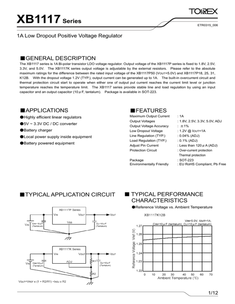
■TYPICAL APPLICATION CIRCUIT
: 1A
: 1.8V, 2.5V, 3.3V, 5.0V, ADJ
: ±1%
: 1.2V @ IOUT=1A
: 0.04% (ADJ)
: 0.1% (ADJ)
: Less than 120μA (ADJ)
: Over-current protection
Thermal protection
: SOT-223
: EU RoHS Compliant, Pb Free
■ TYPICAL PERFORMANCE
CHARACTERISTICS
●Reference Voltage vs. Ambient Temperature
1/12
XB1117 Series
■PIN CONFIGURATION
SOT-223
(TOP VIEW)
■PIN ASSIGNMENT
PIN NUMBER
PIN NAME
FUNCTIONS
1
2
3
ADJ/GND
VOUT
VIN
ADJ/Ground
Output
Input
* The electrical potential of the package fin is the same as the VOUT pin.
■PRODUCT CLASSIFICATION
●Ordering Information
XB1117①②③④⑤⑥-⑦
DESIGNATOR
ITEM
①
Type of Regulators
②③④
⑤⑥-⑦(*1)
(*1)
2/12
SYMBOL
DESCRIPTION
P
Fixed VOUT type
K
Adjustable VOUT type
181
Fixed VOUT 1.80V (±1%)
251
Fixed VOUT 2.50V (±1%)
331
Fixed VOUT 3.30V (±1%)
501
Fixed VOUT 5.00V (±1%)
12B
Adjustable VOUT 1.25V (±1%)
Output Voltage
& Accuracy
Package
(Order Unit)
FR-G
SOT-223(1,000/Reel)
The “-G” suffix denotes Halogen and Antimony free as well as being fully EU RoHS compliant.
XB1117
Series
■BLOCK DIAGRAM
3/12
XB1117 Series
■ABSOLUTE MAXIMUM RATINGS
XB1117P501
PARAMETER
SYMBOL
RATINGS
UNITS
Input Voltage
Thermal Resistance
(Junction to Case)
Thermal Resistance
(Junction to Ambient)
Power Dissipation
(ΔT=100℃)
Operating Ambient Temperature
Operating Junction Temperature Range
Storage Temperature Range
Lead Temperature
VIN
10.0
V
θJC
15
θJA
160
PD
625
mW
Topr
Tj
Tstg
Tlead
0 ~+70
0 ~+125
- 65 ~+150
260
℃
℃/W
*Stress above the listed absolute maximum rating may cause permanent damage to the device.
** The rated values of the XB1117P18 / 25 / 30 (VOUT=1.8V, 2.5V and 3.0V) and XB1117K type are different from that
of the XB1117P50 (VOUT=5.0V).
■ELECTRICAL CHARACTERISTICS
XB1117P501
Ta=25℃
PARAMETER
SYMBOL
Output Voltage
VOUT
Line Regulation
ΔVOUT1
Load Regulation
ΔVOUT2
Dropout Voltage
Vdif
Current Limit
ILIM
Supply Current
ISS
Temperature
Coefficient
TC
Temperature Stability
TS
CONDITIONS
VIN=7.0V
IOUT=0A
7.0V≦VIN≦9.0V
IOUT=0A
VIN=7.0V
0A≦IOUT≦1.0A
ΔVOUT=±1%
0A≦IOUT≦1.0A
7.0V≦VIN≦10.0V
VIN=7.0V
0A≦IOUT≦1.0A
7.0V≦VIN≦10.0V
0A≦IOUT≦1.0A
VIN=7.0V
IOUT=100mA
*Over Temp. = Over Temperature(0~+70℃)
4/12
MIN.
TYP.
MAX.
UNITS
*Over Temp.
4.950
4.900
5.000
5.000
5.050
5.100
V
*Over Temp.
-
1
6
*Over Temp.
*Over Temp.
1.0
5.0
10.1
1.2
1.3
1.5
15.2
20.2
1.4
-
*Over Temp.
-
6
13
mA
-
50
-
ppm/℃
-
0.5
-
%
*Over Temp.
*Over Temp.
mV
V
A
XB1117
Series
■ABSOLUTE MAXIMUM RATINGS
XB1117P181, P251, P331, K12B
PARAMETER
SYMBOL
RATINGS
UNITS
Input Voltage
Thermal Resistance
(Junction to Case)
Thermal Resistance
(Junction to Ambient)
Power Dissipation (ΔT=100℃)
VIN
7.0
V
θJC
15
θJA
160
PD
TOPR
TJ
TSTG
TLEAD
625
0 ~ 70
0 ~ 125
-65 ~ 150
260
Operating Ambient Temperature
Operating Temperature Range
Storage Temperature Range
Lead Temperature
℃/W
mW
℃
*Stress above the listed absolute maximum rating may cause permanent damage to the device.
■ELECTRICAL CHARACTERISTICS
XB1117P181
TJ=25℃
PARAMETER
SYMBOL
Output Voltage
VOUT
Line Regulation
ΔVOUT1
Load Regulation
ΔVOUT2
Dropout Voltage
Vdif
Current Limit
ILIM
Supply Current
ISS
Temperature
Coefficient
TC
Temperature Stability
TS
CONDITIONS
VIN=5.0V
IOUT=0A
MIN.
TYP.
MAX.
UNITS
1.782
1.800
1.818
V
-
1.0
5.5
mV
*Over Temp.
*Over Temp.
1.0
1.80
3.70
1.2
1.3
1.5
18.2
22.0
1.4
-
*Over Temp.
-
6
13
mA
50
-
ppm/
℃
0.5
-
%
*Over Temp.
4.75V≦VIN≦7.0V
IOUT = 0A
VIN=5.0V
0A≦IOUT≦1.0A
ΔVOUT=±1%
0A≦IOUT≦1.0A
4.75V≦VIN≦7.0V
VIN=5.0V
0A≦IOUT≦1.0A
4.75V≦VIN≦7.0V
0A≦IOUT≦1.0A
VIN=5.0V
IOUT=100mA
*Over Temp.
*Over Temp.
-
mV
V
A
*Over Temp. = Over Temperature (0~+70℃)
XB1117P251
TJ =25℃
PARAMETER
SYMBOL
Output Voltage
VOUT
Line Regulation
ΔVOUT1
Load Regulation
ΔVOUT2
Dropout Voltage
Vdif
Current Limit
ILIM
Supply Current
ISS
Temperature
Coefficient
TC
Temperature Stability
TS
STANDARD VALUE
MIN.
TYP.
MAX.
CONDITIONS
VIN=5.0V
IOUT=0A
4.75V≦VIN≦7.0V
IOUT=0A
VIN=5.0V
0A≦IOUT≦1.0A
ΔVOUT=±1%
0A≦IOUT≦1.0A
4.75V≦VIN≦7.0V
VIN=5.0V
0A≦IOUT≦1.0A
4.75V≦VIN≦7.0V
0A≦IOUT≦1.0A
VIN=5.0V
IOUT=100mA
UNITS
2.475
2.450
2.500
2.500
2.525
2.550
V
-
1.0
6.8
mV
*Over Temp.
*Over Temp.
1.0
2.5
5.1
1.2
1.3
1.5
25.3
30.3
1.4
-
*Over Temp.
-
6
13
mA
-
50
-
ppm/
℃
-
0.5
-
%
*Over Temp.
*Over Temp.
*Over Temp.
mV
V
A
*Over Temp. = Over Temperature (0~+70℃)
5/12
XB1117 Series
■ELECTRICAL CHARACTERISTICS (Continued)
XB1117P331
TJ =25℃
PARAMETER
SYMBOL
CONDITIONS
Output Voltage
VOUT
Line Regulation
ΔVOUT1
4.75V≦VIN≦7.0V
IOUT=0A
Load Regulation
ΔVOUT2
VIN=5.0V
0A≦IOUT≦1.0V
Dropout Voltage
Vdif
ΔVOUT=±1%
0A≦IOUT≦1.0A
Current Limit
ILIM
Supply Current
ISS
Temperature
Coefficient
TC
Temperature Stability
TS
VIN=5.0V
IOUT=0A
MIN.
TYP.
MAX.
UNITS
3.267
3.234
3.300
3.300
3.333
3.366
V
-
1.0
4.5
*Over Temp.
*Over Temp.
1.0
3.4
6.7
1.2
1.3
1.5
10.0
13.4
1.4
-
*Over Temp.
-
6
13
mA
-
50
-
ppm/℃
-
0.5
-
%
*Over Temp.
*Over Temp.
4.75V≦VIN≦7.0V
VIN=5.0V
0A≦IOUT≦1.0A
4.75V≦VIN≦7.0V
0A≦IOUT≦1.0A
VIN=5.0V
IOUT=100mA
*Over Temp.
mV
V
A
*Over Temp. = Over Temperature (0~+70℃)
TJ=25℃
XB1117K12B
PARAMETER
SYMBOL
Reference voltage
Vref
Line Regulation
ΔVOUT1
Load Regulation
ΔVOUT2
Dropout Voltage
Vdif
Current Limit
Temperature
Coefficient
ILIM
Adjust Pin Current
IADJ
Adjust Pin Current
Change
ΔIADJ
Temperature Stability
TS
Minimum Load
Current
IOUT
TC
CONDITIONS
VIN=5.0V
IOUT=10mA
4.75V≦VIN≦7.0V
IOUT=0A
VIN=5.0V
10mA≦IOUT≦1.0A
ΔVOUT=±1%
10mA≦IOUT≦1.0A
2.75A≦VIN≦7.0V
2.75V≦VIN≦7.0V
10mA≦IOUT≦1.0A
2.75V≦VIN≦7.0V
10mA≦IOUT≦1.0A
2.75V≦VIN≦7.0V
10mA≦IOUT≦1.0A
VIN=5.0V
IOUT=100mA
VOUT=5.0V
*Over Temp. = Over Temperature (0~+70℃)
6/12
MIN.
TYP.
MAX.
UNITS
1.238
1.225
1.250
1.250
1.262
1.275
V
-
0.04
0.20
%
1.0
0.1
0.2
1.2
1.3
1.5
0.3
0.4
1.4
-
-
50
-
*Over Temp.
-
55
-
120
μA
*Over Temp.
-
0.2
5.0
μA
*Over Temp.
-
0.5
-
%
-
-
10
mA
*Over Temp.
*Over Temp.
*Over Temp.
*Over Temp.
%
V
A
ppm/
℃
XB1117
Series
■OPERATIONAL EXPLANATION
1. Output voltage adjustment
The XB1117 series provide a stable output by comparing the output voltage to an internal reference voltage. With the
adjustable XB1117K type, a 1.25V reference voltage (VREF) is fixed between the VOUT pin and the ADJ pin and the external
resistors R1 and R2 are used to set the output voltage. The resistance values of R1 and R2 should be set so as to provide a
minimum load current of 10mA. The output voltage is given by the following equation.
VOUT=VREF(1+R2/R1)+IADJ x R2
The output voltage of the XB1117P type is internally fixed to 1.8V, 2.5V, 3.3V, and 5.0V so external resistors are not
necessary.
2. Stability and load regulation
The XB1117 series requires a load capacitor between the VOUT pin and the GND pin to provide phase compensation thereby
ensuring stability of the output voltage. Either a tantalum capacitor of more than 10μF (TYP.) or an aluminum electrolytic
capacitor of more than 50μF (TYP.) should be connected.
(Note : The capacitor's ESR value should not exceed 0.5Ω.)
The output capacitor does not have a theoretical upper limit so increasing its value will increase stability. CL=100μF or
more is typical for high current regulator design.
In order to avoid any reductions in output voltage accuracy with the XB1117K type, we recommend not to place a parasitic
resistor (Rp) between the VOUT pin and the divider resistor R1. The parasitic resistor (Rp) does not influence the output
however if the divider resistor R1 is directly connected to the VOUT pin.
With the XB1117P type, although external resistor (R1) is internally connected to the VOUT pin, stability can be maintained by
not wiring a parasitic resistor to the GND pin.
7/12
XB1117 Series
■OPERATIONAL EXPLANATION (Continued)
3. Thermal protection
XB1117 series has thermal protection which limits junction temperature to 150℃. However, device functionally is only
guaranteed to a maximum junction temperature of + 125℃. The power dissipation and junction temperature for the XB1117
series are given by;
PD=(VIN-VOUT) x IOUT
TJ=TA+(PD×θJA)
NOTE:TJ must not exceed 125℃.
4. Current limit protection
XB1117 series is protected against overload conditions. Current protection is triggered at 1.5A (TYP.).
5. Thermal consideration
The XB1117 series contain thermal limiting circuitry designed to protect itself from over-temperature conditions. Even for
normal load conditions, maximum junction temperature ratings must not be exceeded. As mentioned in thermal protection
section, we need to consider all sources of thermal resistance between junction and ambient. It includes junction-to-case,
case-to-heat-sink interface and heat sink thermal resistance itself.
Junction-to-case thermal resistance is specified from the IC junction to the bottom of the case directly below the die. Proper
mounting is required to ensure the best possible thermal flow from this area of the package to the heat sink. The case of all
devices in this product series is electrically connected to the output. Therefore, if the case of the device is not electrically
isolated, a thermally conductive spacer is recommended.
■NOTES ON USE
1. For the phenomenon of temporal and transitional voltage decrease or voltage increase, the IC may be damaged or
deteriorated if IC is used beyond the absolute MAX. specifications.
2. Torex places an importance on improving our products and their reliability.
We request that users incorporate fail-safe designs and post-aging protection treatment when using Torex products in their
systems.
■APPLICATION CIRCUITS
●Adjustable Output Voltage
8/12
XB1117
Series
■APPLICATION CIRCUITS (Continued)
●Regulator with reference voltage
●Regulator with reverse diode protection
9/12
XB1117 Series
■TYPICAL PERFORMANCE CHARACTERISTICS
(1) Load Regulation vs. Ambient Temperature
(2) Reference Voltage vs. Ambient Temperature
(3) Output Short Circuit Current vs. Dropout Voltage
(4) Dropout Voltage vs. Output Current
(5) Adjust Pin Current vs. Ambient Temperature
(6) Supply Current vs. Dropout Voltage
(7) Load Transient Response
10/12
(8) Line Transient Response
XB1117
Series
■ PACKAGING INFORMATION
●SOT-223
■MARKING RULE
●SOT-223
① represents product series
MARK
B
PRODUCT SERIES
XB1117xxxxFx
② represents fixed or adjustable output voltage
MARK
K
P
PRODUCT SERIES
XB1117KxxxFx
XB1117PxxxFx
③ represents output voltage
SOT-223
(TOP VIEW)
MARK
B
K
T
2
M
OUTPUT VOLTAGE (V)
ADJ
1.8
2.5
3.3
5.0
PRODUCT SERIES
XB1117K12BFx
XB1117P181Fx
XB1117P251Fx
XB1117P331Fx
XB1117P501Fx
④ represents production lot number
0 to 9, A to Z repeated. (G, I, J, O, Q, W are excepted.)
11/12
XB1117 Series
1. The products and product specifications contained herein are subject to change without
notice to improve performance characteristics.
Consult us, or our representatives
before use, to confirm that the information in this datasheet is up to date.
2. We assume no responsibility for any infringement of patents, patent rights, or other
rights arising from the use of any information and circuitry in this datasheet.
3. Please ensure suitable shipping controls (including fail-safe designs and aging
protection) are in force for equipment employing products listed in this datasheet.
4. The products in this datasheet are not developed, designed, or approved for use with
such equipment whose failure of malfunction can be reasonably expected to directly
endanger the life of, or cause significant injury to, the user.
(e.g. Atomic energy; aerospace; transport; combustion and associated safety
equipment thereof.)
5. Please use the products listed in this datasheet within the specified ranges.
Should you wish to use the products under conditions exceeding the specifications,
please consult us or our representatives.
6. We assume no responsibility for damage or loss due to abnormal use.
7. All rights reserved. No part of this datasheet may be copied or reproduced without the
prior permission of TOREX SEMICONDUCTOR LTD.
12/12


