Active PFC Boost Rectifier
advertisement

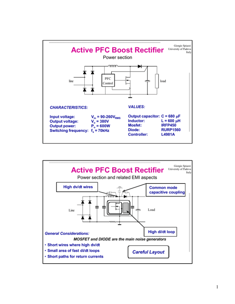
Active PFC Boost Rectifier Giorgio Spiazzi University of Padova Italy Power section PFC Control line VALUES: CHARACTERISTICS: Input voltage: Output voltage: Output power: Switching frequency: load Vin = 90-260VRMS Vo = 380V Po = 600W fs = 70kHz Output capacitor: Inductor: Mosfet: Diode: Controller: C = 680 µF L = 600 µH IRFP450 RURP1560 L4981A Active PFC Boost Rectifier Giorgio Spiazzi University of Padova Italy Power section and related EMI aspects High dv/dt wires Line Common mode capacitive coupling Load High di/dt loop General Considerations: MOSFET and DIODE are the main noise generators • Short wires where high dv/dt • Small area of fast di/dt loops Careful Layout • Short paths for return currents 1 Circuit Layout (components) Giorgio Spiazzi University of Padova Italy Output Input Power stage Output filter Input filter Control and drive Active PFC Boost Rectifier Circuit Layout (solder layer) Giorgio Spiazzi University of Padova Italy 2 Active PFC Boost Rectifier Circuit Layout (component layer) Active PFC Boost Rectifier Circuit Layout Considerations Giorgio Spiazzi University of Padova Italy Giorgio Spiazzi University of Padova Italy Short paths among switching components and filter capacitor MOS High dv/dt track is short ... D ... and shielded between +Vout and -Vout tracks 3 Active PFC Boost Rectifier Circuit Layout Considerations Giorgio Spiazzi University of Padova Italy Shielding tracks connected to reference Small area of the gate circuit. Snubber close to gate and source terminals Control Short (and shielded) track at analog inputs Active PFC Boost Rectifier Circuit Layout Considerations Giorgio Spiazzi University of Padova Italy Shield plane connected to reference Star connection of ground paths Common mode filter capacitors 4 Active PFC Boost Rectifier Giorgio Spiazzi University of Padova Italy Power section with EMI Filters Low CM impedance High CM impedance i cm Coupled inductors show high common mode inductance but low differential mode inductance: i dm Ex: 6.8 mH CM, 70 µH DM Active PFC Boost Rectifier Giorgio Spiazzi University of Padova Italy Input filter design - Differential Mode Lcm = 6.8 mH Ripple amplitude ∆I max = U out ≅ 113 . A 8 fs L L dm = 70 µH vn 50 Ω i dm 50 Ω triangular waveform Differential mode input noise: 70 kHz, (peak values) 140 kHz, 210 kHz, 280 kHz, 350 kHz, 420 kHz, 1 µF 2 µF 87 dB µV 57 dB µV 40 dB µV 26 dB µV 19 dB µV 9 dB µV a suitable margin (20 dB µV) is maintained for the commom mode noise and possible resonances 5 Active PFC Boost Rectifier Giorgio Spiazzi University of Padova Italy Input filter design - Common Mode i cm i cm L cm = 6.8 mH 100 nF 4.7 nF 50 Ω 4.7 nF 1 µF 2 µF • • • • Several current return paths are present The main one is on the output side of the PFC High value of filter inductor reduces current term at the input side CM input side current generates DM input noise due to asymmetrical converter topology • Adding CM capacitors at the input side reduces input CM voltage noise but the increased CM current causes additional DM noise Prototype Tests Giorgio Spiazzi University of Padova Italy Input behavior Line Voltage v i 100 V/div. 2 A/div. Line current 6 Giorgio Spiazzi University of Padova Italy Prototype Tests Line Voltage and Inductor Current (peak to peak sampling) Inductor current switching ripple v iL Giorgio Spiazzi University of Padova Italy Prototype Tests Gate drive circuit IL+ID threshold iL Voltage drop vDS vG iD vGS IL threshold 7 Giorgio Spiazzi University of Padova Italy Prototype Tests Gate drive circuit iL vG iD vDS vGS IL threshold Commutation is sloweddown Giorgio Spiazzi University of Padova Italy Prototype Tests Gate drive circuit vDS Drain-Gate coupling iG vG iD vGS 8 Giorgio Spiazzi University of Padova Italy Prototype Tests Gate drive circuit vDS iG vG iD vGS Prototype Tests Giorgio Spiazzi University of Padova Italy Modulation of Switching Frequency VDS Spectra Modulated Fixed 9 Prototype EMI Tests Giorgio Spiazzi University of Padova Italy Conducted noise (peak measure) Neutral Phase Prototype EMI Tests Conducted noise (peak measure) Giorgio Spiazzi University of Padova Italy Introducing input-side common-mode filter capacitors • Differential noise increases (circuit is not symmetrical) and low-frequency behavior is worse • A resonance, between input and output CM filter capacitors and the inductances of their connections, appears, modifying the highfrequency behavior Added Line PFC 10 Prototype EMI Tests Giorgio Spiazzi University of Padova Italy Conducted noise (peak measure) Increased output-side common-mode capacitors • Common mode currents are closed on the output side (no additional voltage drop on the input filter occurs) • Low-frequency behavior is improved • High-frequency behavior becomes worse due to resonance of two CM filter capacitors and their connections Added PFC Load Prototype EMI Tests Giorgio Spiazzi University of Padova Italy Conducted noise (peak measure) By connecting the heatsink to the negative rail (capacitive currents are closed “near” to the Mosfet source): •Low-frequency behaviour is improved •High-frequency behavior is good (the heatsink shields all circuitry) 11 Prototype EMI Tests Conducted noise (peak measure) Giorgio Spiazzi University of Padova Italy By inserting a shield, between Mosfet and heatsink, connected to Mosfet source (drain coupled capacitive currents are closed directly to the Mosfet source) •Low-frequency behavior is improved (common mode noise is reduced) •High-frequency behavior is good (Using the heatsink as shield of the whole circuit gives however better results) Shield Prototype EMI Tests Giorgio Spiazzi University of Padova Italy Conducted noise (peak measure) Switching Frequency Modulation Switching frequency harmonic components disappear • Measured peak noise remains unchanged • Measured average noise is considerably reduced Peak Average 12 Prototype EMI Tests Giorgio Spiazzi University of Padova Italy Conducted noise (peak measure) Effect of Diode Reverse Recovery (Disconnecting gate snubber) • Low-frequency behavior is almost unchanged • High-frequency behavior is heavily worsened iL vG iD Prototype EMI Tests Giorgio Spiazzi University of Padova Italy Conducted noise (peak measure) Increasing gate resistor • Low-frequency behavior remains unchanged • High-frequency behavior is improved (MOSFET commutation slows down) iG 33 vG iD 72 Ω 13 Prototype EMI Tests Giorgio Spiazzi University of Padova Italy By spreading the ac wires close to the input filter (filter inductors inside plastic can) •Low-frequency behavior becomes worse (input wires capture leakage magnetic field of filter inductor) •High-frequency behavior remains unchanged Line EMI Filter PFC Increased Area 14
