AN579
Application note
Protection concepts in telecommunications equipment
Introduction
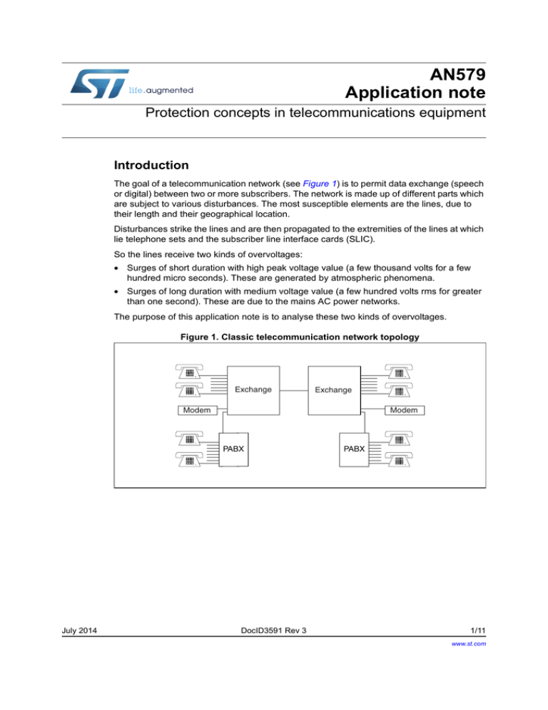
The goal of a telecommunication network (see Figure 1) is to permit data exchange (speech
or digital) between two or more subscribers. The network is made up of different parts which
are subject to various disturbances. The most susceptible elements are the lines, due to
their length and their geographical location.
Disturbances strike the lines and are then propagated to the extremities of the lines at which
lie telephone sets and the subscriber line interface cards (SLIC).
So the lines receive two kinds of overvoltages:
• Surges of short duration with high peak voltage value (a few thousand volts for a few
hundred micro seconds). These are generated by atmospheric phenomena.
• Surges of long duration with medium voltage value (a few hundred volts rms for greater
than one second). These are due to the mains AC power networks.
The purpose of this application note is to analyse these two kinds of overvoltages.
Figure 1. Classic telecommunication network topology
Exchange
Exchange
Modem
Modem
PABX
July 2014
DocID3591 Rev 3
PABX
1/11
www.st.com
11
Overvoltages across telecommunication lines
AN579
1
Overvoltages across telecommunication lines
1.1
Atmospheric effects
Lightning phenomena are the most common surge causes. They are mainly due to a
voltage difference between the ground and the clouds (a few 100 kV). Two kinds of strikes
may occur:
•
Negative discharge with a peak current of 50 kA, rise time of 10 µs to 15 µs and 100 µs
duration
•
Positive discharge with a peak value of 150 kA, rise time between 20 µs and 50 µs and
a duration between 100 ms and 200 ms
The lightning effect appears on the lines in two ways.
•
Direct shock
•
Induced shock
Figure 2. Lightning phenomenon
Ionoshere
+++++++
Cloud
- - - - - - -
Ground
Figure 3. Direct lightning strike
1
2
Central
Office
3
4
5
6
7
8
9
*
0
#
Figure 3 shows the first case which is produced mainly on overhead lines.
2/11
DocID3591 Rev 3
AN579
Overvoltages across telecommunication lines
Induced shock is more frequent than a direct shock. Lightning strikes the ground and a
current flows in the cable shield. This current produces a voltage gradient which in some
places is above the insulation capability of the cable material (see Figure 4).
Figure 4. Direct lightning strike
Subscriber
1
1.2
2
Central
Office
3
4
5
6
7
8
9
*
0
#
Proximity and crossing with AC mains lines
For these kinds of surges two cases may be seen:
•
AC mains cable fallen on a telephone line
•
Proximity of a subcriber line with an AC mains line or equipment (mainly capacitive
coupling)
Typically these events create disturbances with an rms value of a few amperes for a
duration of between 1 s and 15 min.
DocID3591 Rev 3
3/11
11
Primary and secondary protection
2
AN579
Primary and secondary protection
Figure 2, Figure 3 and Figure 4 give us an idea of the energy which may appear on the
lines. In the field these surge values are lower due to the losses of ground resistance, the
capacitive coupling and so on, but are signifiant nevertheless.
We have to divide these disturbances into two families:
•
High peak value and short duration (lightning)
•
Reduced peak value and long duration (crossing with AC power)
For both cases the present state of the art of silicon protection devices does not permit the
suppression of these levels of energy.
A second parameter to keep in mind is the very low clamping factor needed by the IC’s used
to realize the line interface. The clamping factor is the ratio of the normal operating voltage
over the maximum clamping voltage. This forces the designer to use a protection solution
with silicon (fast response time/low clamping factor).
SLIC
Secondary
Protection
Line
Primary
Protection
Figure 5. Primary/secondary protection topology
High energy values and low clamping factor impose two protection levels.
The first level called primary protection (see Figure 5), located on the connecting terminal of
the exchange, suppresses the major part of the disturbance. The second level called
secondary protection reduces the remaining overvoltage.
4/11
DocID3591 Rev 3
AN579
Primary and secondary protection
Figure 6. Primary/secondary protection topology resukts
V peak
>
20 kV
A
t > 50 ms
B
1 to 4 kV
t < 1ms
C
Few 10 V
A: Overvoltage across the line without protection.
B: Remaining voltage after the primary level action.
C: Remaining voltage after the secondary level action.
Figure 6 shows the goal of both protection levels.
In this example the surge across the line without protection will be several 10s of kV peak
value for several 10 ms duration (Figure 6A).
After the primary protection the major part of the energy is eliminated (Figure 6B). The
remaining overvoltage may be a few kV (depending on the dv/dt of the surge and the surge
arrestor technology used).
Across the second level protection the voltage does not exceed a few 10s of volts.
2.1
Primary protection
Two kinds of primary protection are used:
•
Carbon gaps
•
Gas tubes
Figure 7. Carbon gap based primary protection
Zl
Line
Exchange
Zl
DocID3591 Rev 3
5/11
11
Primary and secondary protection
2.1.1
AN579
Carbon gaps
These components are made by two carbon electrodes. The carbon gap is a low cost
primary protection but it has two major disadvantages:
•
short life duration
•
variable spark threshold
Figure 8. Carbon gap based primary protection
Zl
Line
Exchange
Zl
2.1.2
Gas tubes
These components are made of two metallic electrodes in a sealed case. Generally the
sealed tub contains a low pressure gas.
Figure 9. Gas tube characteristics
V
1
2
3
1: Sparkover voltage.
2: Glow discharge voltage.
3: Remaining voltage in switch on mode.
The major disadvantage of this kind of device is its response time, in fact the maximum
voltage across the gas tube depends on the dv/dt of the surge.
6/11
DocID3591 Rev 3
AN579
2.2
Primary and secondary protection
Secondary protection
Figure 10. Series and parallel protection
1
2
Module
to be
protected
1: Series protection.
2: Parallel protection.
The secondary protection level is generally achieved with two types of devices:
2.2.1
•
The series protection ensures protection against the proximity of or the crossing with
AC power lines.
•
The parallel protection operates to suppress the overvoltages due to the lightning
effects.
Series devices
Series devices operate either by:
•
opening the circuit (fuse)
•
an increment of the resistance (PTC)
Figure 11. Fuse protection
Fuse
Exchange
Line
Fuse
The fuse is a classical case of protection by opening the circuit. Figure 11 shows an
exchange protected by fuses and Figure 12 represents an example of the limit curve of the
fusing action.
DocID3591 Rev 3
7/11
11
Primary and secondary protection
AN579
Figure 12. Fuse blowing results
t (s)
100
2.5A
10
1
.1
.01
1
100
10
I (A)
These components provide an absolute security after action, but their major disadvantage is
the need for maintenance.
Figure 13. PTC based protection
PTC
Is
PP
Exchange
Line
PP
PTC
The PTC thermistor is a device which operates through a very rapid resistance increase as
a function of the temperature.
When the surge occurs across the line, the parallel protection PP is activated.
The surge current Is, generated by PP action, flows through the PTC device and increases
its internal temperature. As shown in Figure 14 the resistance value of the PTC device rises
quickly with the temperature.
Figure 14. PTC based protection results
R (Ω)
100k
10k
1k
100
10
25
150
t (˚C)
The major disadvantage of the fuse does not exist with the PTC device. Unfortunately this
kind of component has a large tolerance, a long time to return to its stand off point and a drift
of its value.
Another series device is the simple resistance which limits the current through the parallel
protection device.
8/11
DocID3591 Rev 3
AN579
2.2.2
Conclusion
Parallel devices
The parallel protection function may be assumed by different devices based on different
technologies.
In fact it is clear that the future in term of SLIC topology is based on the use of ICs. So the
consequent requirement for good response times and high clamping factor necessitates the
use of silicon protection.
Parallel silicon protection functions in two different modes:
3
•
The clamping mode with the Transil™
•
The crowbar mode with the Trisil™
Conclusion
Due to atmospheric effects and disturbances on mains networks, telecommunication lines
have to be protected. Due to the improvement in telecommunication system technology, a
need for fast and precise protection solutions results.
The choice of the protection technique will be made considering local standards and the
technology of the devices to be protected.
This protection will be assumed to be dual level:
•
Primary level to suppress high energy
•
Secondary level to optimize the remaining overvoltage
TM: Transil and Trisil are trademarks of STMicroelectronics
DocID3591 Rev 3
9/11
11
Revision history
4
AN579
Revision history
Table 1. Document revision history
10/11
Date
Revision
Changes
March-1993
1
First Issue
19-Apr-2004
2
Stylesheet update. No content change.
28-Jul-2014
3
Updated trademark statements.
DocID3591 Rev 3
AN579
IMPORTANT NOTICE – PLEASE READ CAREFULLY
STMicroelectronics NV and its subsidiaries (“ST”) reserve the right to make changes, corrections, enhancements, modifications, and
improvements to ST products and/or to this document at any time without notice. Purchasers should obtain the latest relevant information on
ST products before placing orders. ST products are sold pursuant to ST’s terms and conditions of sale in place at the time of order
acknowledgement.
Purchasers are solely responsible for the choice, selection, and use of ST products and ST assumes no liability for application assistance or
the design of Purchasers’ products.
No license, express or implied, to any intellectual property right is granted by ST herein.
Resale of ST products with provisions different from the information set forth herein shall void any warranty granted by ST for such product.
ST and the ST logo are trademarks of ST. All other product or service names are the property of their respective owners.
Information in this document supersedes and replaces information previously supplied in any prior versions of this document.
© 2014 STMicroelectronics – All rights reserved
DocID3591 Rev 3
11/11
11


