Properties
Copper Foils for High Frequency
Materials
Copper foils, for the wide range of Rogers’ high frequency circuit substrates, are designed to provide
optimum performance in high reliability applications.
There are various types of copper foil are offered; in a range of weights (thicknesses). Their
characteristics differ, and an understanding of these differences is important to ensure the correct
selection of copper foil for each application or environmental condition.
Copper Foil Manufacturing
Standard ED Copper
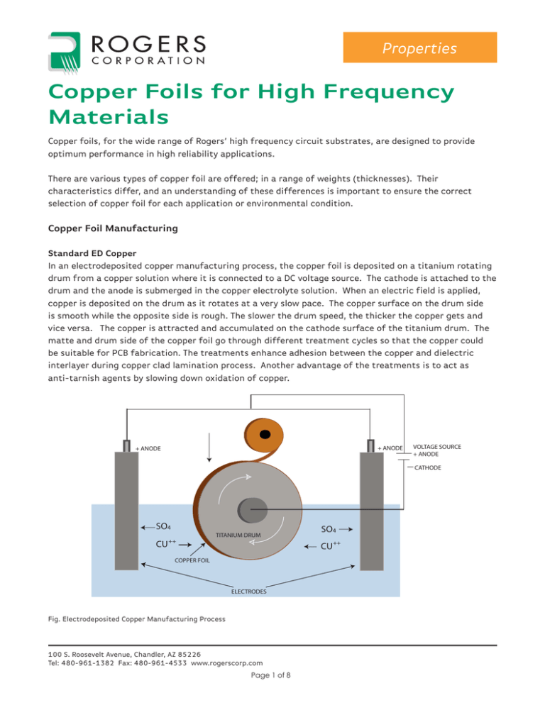
In an electrodeposited copper manufacturing process, the copper foil is deposited on a titanium rotating
drum from a copper solution where it is connected to a DC voltage source. The cathode is attached to the
drum and the anode is submerged in the copper electrolyte solution. When an electric field is applied,
copper is deposited on the drum as it rotates at a very slow pace. The copper surface on the drum side
is smooth while the opposite side is rough. The slower the drum speed, the thicker the copper gets and
vice versa. The copper is attracted and accumulated on the cathode surface of the titanium drum. The
matte and drum side of the copper foil go through different treatment cycles so that the copper could
be suitable for PCB fabrication. The treatments enhance adhesion between the copper and dielectric
interlayer during copper clad lamination process. Another advantage of the treatments is to act as
anti-tarnish agents by slowing down oxidation of copper.
+ ANODE
+ ANODE
VOLTAGE SOURCE
+ ANODE
CATHODE
SO4
CU
++
TITANIUM DRUM
COPPER FOIL
ELECTRODES
Fig. Electrodeposited Copper Manufacturing Process
100 S. Roosevelt Avenue, Chandler, AZ 85226
Tel: 480-961-1382 Fax: 480-961-4533 www.rogerscorp.com
Page 1 of 8
SO4
CU ++
Rolled Copper
Rolled copper is made by successive cold rolling operations to reduce thickness and extend length starting with a
billet of pure copper. The surface smoothness depends on the rolling mill condition.
Reducing Rolls
Copper
Foil
Copper Billet
Fig. Rolled Copper Manufacturing Process
Resistive Copper
The matte side of the ED copper is coated with metal or alloy that acts as a resistive layer. The next process is to
roughen the resistive layer with nickel particles.
Reverse Treated ED Copper and LoPro Copper Foil
Reverse treated foils involve the treatment of the smooth side of electrodeposited copper. Treatment layers are
thin coatings that improve adhesion of the base foil to dielectrics and add corrosion resistance which makes the
shiny side rougher than it was before. During the process of making circuit board panels, the treated side of
copper is laminated to the dielectric material. The fact that the treated drum side is rougher than the other side
constitutes a greater adhesion to the dielectric. That is the major advantage over the standard ED copper. The
matte side doesn’t need any mechanical or chemical treatment before applying photoresist. It is already rough
enough for good laminate resist adhesion.
In case of the LoPro™ copper, a thin layer of adhesive is applied on the reverse treated side of the copper. There
is a physical layer of the bond enhancement material. Just like the reverse treated electrodeposited copper,
the adhesive treated side is bonded to the dielectric layer for better adhesion. Our RO4000 series material are
available laminated with LoPro copper foil.
Crystalline Structure
Electrodeposited copper crystals tend to grow lengthwise in the Z-axis of the foil. Typically, a polished section of
electrodeposited copper foil has the appearance of a picket fence, with long crystal boundaries perpendicular to
the foil plane. Rolled copper crystals are broken and crushed during the cold rolling operation. They are smaller
than the electrodeposited crystals, and have irregular, spherical shapes, nearly parallel to the foil plane.
100 S. Roosevelt Avenue, Chandler, AZ 85226
Tel: 480-961-1382 Fax: 480-961-4533 www.rogerscorp.com
Page 2 of 8
Foil Type
Weight or Thickness
Surface Roughness
Rq (m)
Dielectric
Side
Top
Side
1 oz (35m)
0.4
0.3
½ oz. (18 m)
0.4
0.3
1 oz (35 m)
2.1
0.5
½ oz. (18 m)
1.8
0.4
¼ oz. (8.5 m)
0.8
0.4
1 oz (35 m)
2.2
0.4
½ oz. (18 m)
1.7
0.4
2 oz. (70m)
3.3
0.4
1 oz. (35 m)
3.2
0.5
½ oz. (18 m)
2.8
0.4
Rolled
Electrodeposited
Electrodeposited
Low Profile
Reverse Treated
LoPro® Foil
Resistive Foil
18 m
0.5
0.4
12 m
0.5
0.4
9 m
0.5
0.3
1 oz. (35 m)
0.9
1.3
½ oz. (18 m)
0.7
0.8
Products
RO3003™, RO3006™, RO3010™, RO3035™,
RO3203™, RO3206™, RO3210™
RT/duroid® 5870, 5880, 6002, 6202, 6006,
6010LM, ULTRALAM® 2000 laminates
RO3003, RO3006, RO3010, RO3035, RO3203,
RO3206, RO3210
RT/duroid 5870, 5880, 6002, 6202, 6006,
6010LM
ULTRALAM 2000
TMM® 3,4, 6,10, 10i laminates
RT/duroid 6035HTC laminates
RO4003C™, RO4350B™, RO4360™ RO4533™
RO4534™, RO4350B-TX laminates
ULTRALAM 3000, XT/duroid®, laminates
RT/duorid 6035HTC laminates
1 oz. (35 m)
0.6
1.1
½ oz. (18m)
0.5
0.6
RO4003C, RO4350B, RO4533, RO4534,
RO4730™ laminates
TCR® Thin Film Resistor Foil
½ oz. (18m)
2.2
0.5
RO4003C, RO4350B laminates
OhmegaPly®
Resistor-Conductor
Material
25 ohms ½ oz (18 m)
1.4
0.3
RO4003C laminates
1.0
0.3
RO3003 , RO3006, RO3010, RO3035, RO3203,
RO3206, RO3210,
RT/duroid 5870, 5880, 6002, 6202, 6006,
6010LM laminates
OhmegaPly
Resistor-Conductor
Material
25 ohms ½ oz. (18m)
Table 1. Typical Copper Roughness Data
Copper Foil Roughness Measurements
An optical profiler can be used to analyze the three-dimensional surface profile of a copper foil to subsequently
determnie its RMS roughness. RMS or Rq is the “root-mean-squared” roughness calculated over the profiled
area. The surface morphology of half ounce electrodeposited copper on figure 1 clearly shows that the treated
side has granular dendritic structure and the untreated side has a smoother surface.
100 S. Roosevelt Avenue, Chandler, AZ 85226
Tel: 480-961-1382 Fax: 480-961-4533 www.rogerscorp.com
Page 3 of 8
.406m
Fig 1. Wyko® Optical Profiler Surface Morphology and Roughness Measurements of Treated and Untreated
Half Ounce Copper (not to scale)
As displayed on Table 1, roughness data of electrodeposited and rolled copper foils with different thicknesses
was obtained by using an optical surface profiler. It also shows for which products the individual copper foils are
used at Rogers Corporation. The rolled copper with no surface treatment is typically the smoothest.
100 S. Roosevelt Avenue, Chandler, AZ 85226
Tel: 480-961-1382 Fax: 480-961-4533 www.rogerscorp.com
Page 4 of 8
Electric Performance of Laminates
Copper surface roughness can increase conductor loss of a microwave circuit as frequency increases and to
the extent that the signal skin depth is comparable or smaller than the scale of the copper roughness. A
simple explanation of this effect is that the small skin depth signal must travel along the surface of the rough
conductor, effectively increasing the path length and conductor resistance.
There have been many attempts to characterize the relationship between the copper conductor surface
roughness and the losses. Morgan[1] published a paper where numerical modeling was done to approximate the
losses
associated with conductor roughness and in relation to frequency. An example of conductor losses of
.
microstrip transmission lines using different copper roughness and the application of the Morgan rule (labeled
MWI) is shown in figure 2.
ED
Fig 2. Insertion loss 50 ohm microstrip transmission lines with various copper foils on 0.004” ULTRALAM® 3850
laminates.
The above graph shows insertion loss versus frequency for five different copper foils which were laminated
to 0.004” LCP dielectric material. Comparing the treated electrodeposited and rolled copper foils, the rolled
(RMS=0.4mm) treated copper has lower insertion loss. The one with the highest insertion loss is the treated
electrodeposited foil (RMS=2.5mm) whereas the untreated electrodeposited copper with RMS value of 0.3mm
has the lower insertion loss. It can be concluded that the smoother the copper the lower the insertion loss
becomes.
More recently a paper[2] disclosed the relationship between copper roughness and the effect on the phase
constant as well as insertion loss. As part of this work a sophisticated model was developed which very closely
100 S. Roosevelt Avenue, Chandler, AZ 85226
Tel: 480-961-1382 Fax: 480-961-4533 www.rogerscorp.com
Page 5 of 8
approximates measured circuits of varying geometry. This model was developed by Sonnet Software and is an
electromagnetic field solver, using complex impedance. A correlation between this model and measured circuits
is shown in figure 3.
Fig 3. Comparison between EM model and measured microstrip circuits for insertion loss, when accounting for
conductor roughness.
This same study found that copper surface roughness impacts the effective dielectric constant of a microstrip
transmission line and this is done by the roughness having an effect on the propagation constant. A thinner
circuit will be more sensitive to the conductor surface roughness and the effective dielectric constant will
increase with an increase in roughness. This is demonstrated in figure 4.
Fig 4. Comparisons of different copper roughness on the effective dielectric constant of microstrip
transmission lines.
100 S. Roosevelt Avenue, Chandler, AZ 85226
Tel: 480-961-1382 Fax: 480-961-4533 www.rogerscorp.com
Page 6 of 8
Mechanical Performance of Laminates
A.
B.
C.
Thermal Shock Resistance
Under some extreme conditions of rapid thermal cycling, electrodeposited copper may exhibit thermal
stress cracks in narrow conductors. Under similar conditions, rolled copper has significantly improved
resistance to cracking. Although electrodeposited copper has greater tensile strength and elongation
before breaking, rolled copper has better elastic elongation before reaching permanent deformation.
Foil Adhesion
Because the adhesion of resin systems to metals is mechanical, bond strength is directly related to the
surface roughness of the treated foil side. Typical peel strengths after thermal shock for 1 oz. copper foils
to
Bondability of Stripline Assemblies (PTFE Substrates)
The SEM photographs below illustrate the differences in topography and roughness between copper types
and etch dielectric surfaces. If the boards are to be adhesive bonded, then for electrodeposited copper,
sodium etch or plasma etch of the dielectric surface is not necessary, provided that care is exercised to
preserve the surface topography. However, for rolled copper-clad circuit boards, the surface roughness of
the dielectric will give a poor mechanical bond, and surface treatment is necessary for reliable chemically
bonded assemblies.
Fig. 5: SEM images of copper and dielectric
100 S. Roosevelt Avenue, Chandler, AZ 85226
Tel: 480-961-1382 Fax: 480-961-4533 www.rogerscorp.com
Page 7 of 8
Properties
The different manufacturing methods of the two types of foil lead to differences in the electrical and
Mechanical properties. The primary differences are listed in Table 2.
Electrodeposited
Rolled
Property
¼ oz
8 m)
0.5 oz
(18 m)
1 oz.
(35 m)
2 oz
(70 m)
0.5 oz
(18 m)
1 oz.
(35 m)
2 oz.
(70 m)
Tensile Strength, kpsi
15
33
40
40
20
22
28
2
2
3
3
8
13
27
1.66
1.62
1.62
1.78
1.74
1.74
Elongation, %*
Vol Resistivity
Mohm•cm
Table 2. Typical Foil Properties
* Values represent properties after lamination to a PTFE laminate.
Table 3 lists the recommended copper foil type for specific applications or environmental conditions.
Copper Type
Electrodeposited
Rolled
Reverse Treated
High Frequencies
(Low PIM 20 GHz)
X
X
Thermal Shock Environment
X
Mechanical Stress
X
Bonded Assemblies
X
Fine Lines Circuit
(< 5mil traces)
¼ oz. (8.5m)
X
Table 3: Application Recommendations
References:
1.
S. P. Morgan, “Effect of surface roughness on eddy current losses at microwave frequencies,” J. Applied Physics, p. 352, v. 20, 1949
2.
Allen F. Horn III, John W. Reynolds, Patricia A. LaFrance, James C. Rautio, “Effect of conductor profile on the insertion loss, phase
constant, and dispersion in thin high frequency transmission lines”, DesignCon 2010
The information in this data sheet is intended to assist you in designing with Rogers’ circuit material laminates. It is not intended to
and does not create any warranties express or implied, including any warranty of merchantability or fitness for a particular purpose or
that the results shown on this data sheet will be achieved by a user for a particular purpose. The user should determine the suitability
of Rogers’ circuit material laminates for each application.
These commodities, technology and software are exported from the United States in accordance with the Export Administration
regulations. Diversion contrary to U.S. law prohibited.
The Rogers’ logo is a licensed trademark of Rogers Corporation
RO3035, LoPro, XT/duroid, RO4533, RO4534, RO4360, RO3035, RO4730, RT/duroid, ULTRALAM, RO4003C, RO4350B, RO3003, RO3006,
RO3010, RO3203, RO3206, RO3210 and TMM are licensed trademarks of Rogers Corporation
OhmegaPly is a registered trademark of Ohmega Technologies, Inc.
TCR is a registered trademark owned by Nippon Mining & Metals Co., Ltd.
Ticer Technologies is a licensee of the technology and trademark of TCR”
Wyko is a trademark of Veeco Instruments.
© 2015 Rogers Corporation, Printed in U.S.A. All rights reserved.
Revised 1153 040915 Publication #92-243
100 S. Roosevelt Avenue, Chandler, AZ 85226
Tel: 480-961-1382 Fax: 480-961-4533 www.rogerscorp.com
Page 8 of 8
