Unique High Efficiency 12V Converter Operates with Inputs from 6V
advertisement
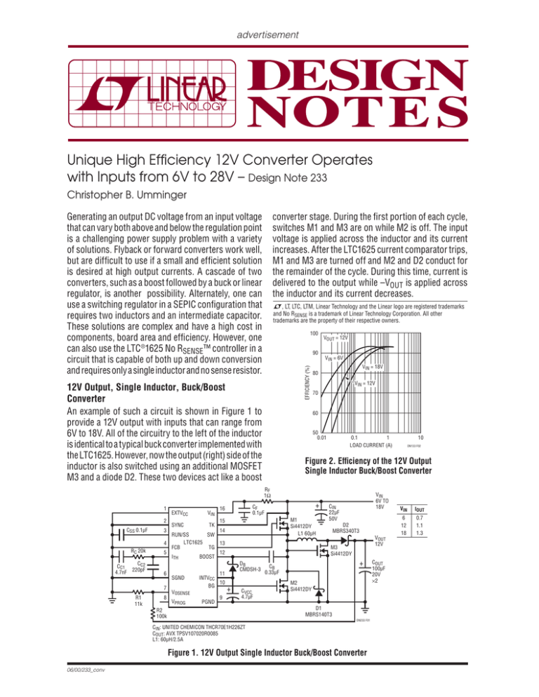
advertisement Unique High Efficiency 12V Converter Operates with Inputs from 6V to 28V – Design Note 233 Christopher B. Umminger Generating an output DC voltage from an input voltage that can vary both above and below the regulation point is a challenging power supply problem with a variety of solutions. Flyback or forward converters work well, but are difficult to use if a small and efficient solution is desired at high output currents. A cascade of two converters, such as a boost followed by a buck or linear regulator, is another possibility. Alternately, one can use a switching regulator in a SEPIC configuration that requires two inductors and an intermediate capacitor. These solutions are complex and have a high cost in components, board area and efficiency. However, one can also use the LTC ®1625 No RSENSE ™ controller in a circuit that is capable of both up and down conversion and requires only a single inductor and no sense resistor. converter stage. During the first portion of each cycle, switches M1 and M3 are on while M2 is off. The input voltage is applied across the inductor and its current increases. After the LTC1625 current comparator trips, M1 and M3 are turned off and M2 and D2 conduct for the remainder of the cycle. During this time, current is delivered to the output while –VOUT is applied across the inductor and its current decreases. L, LT, LTC, LTM, Linear Technology and the Linear logo are registered trademarks and No RSENSE is a trademark of Linear Technology Corporation. All other trademarks are the property of their respective owners. 100 EFFICIENCY (%) 90 12V Output, Single Inductor, Buck/Boost Converter An example of such a circuit is shown in Figure 1 to provide a 12V output with inputs that can range from 6V to 18V. All of the circuitry to the left of the inductor is identical to a typical buck converter implemented with the LTC1625. However, now the output (right) side of the inductor is also switched using an additional MOSFET M3 and a diode D2. These two devices act like a boost VOUT = 12V VIN = 6V VIN = 18V 80 VIN = 12V 70 60 50 0.01 0.1 1 LOAD CURRENT (A) Figure 2. Efficiency of the 12V Output Single Inductor Buck/Boost Converter RF 1Ω 1 2 RC 20k CC1 4.7nF CC2 220pF TK 16 M1 Si4412DY L1 60μH 15 3 14 RUN/SS SW LTC1625 4 13 FCB TG 5 12 ITH BOOST 6 7 R1 11k SYNC VIN + CF 0.1μF 8 SGND INTVCC BG VOSENSE VPROG PGND DB CMDSH-3 11 10 9 VIN 6V TO 18V CIN 22μF 50V D2 MBRS340T3 VOUT 12V M3 Si4412DY + CSS 0.1μF EXTVCC CVCC 4.7μF + CB 0.33μF M2 Si4412DY D1 MBRS140T3 R2 100k DN233 F01 CIN: UNITED CHEMICON THCR70E1H226ZT COUT: AVX TPSV107020R0085 L1: 60μH/2.5A Figure 1. 12V Output Single Inductor Buck/Boost Converter 06/00/233_conv 10 DN133 F02 COUT 100μF 20V w2 VIN IOUT 6 12 18 0.7 1.1 1.3 The duty cycle for the Figure 1 circuit is equal to VOUT/ (VIN + VOUT ). When VIN is equal to VOUT, a fifty percent duty cycle is required to balance the volt-seconds across the inductor. Both the input and output capacitors must filter a square pulse current in this topology. The average value of the inductor current is equal to the sum of the input and output currents. Since the LTC1625 uses MOSFET VDS sensing to control the inductor current peaks, the output current limit depends upon the duty cycle and will vary with the input voltage. At VIN = 12V, the maximum output current is about 1.1A. Efficiency of the circuit is shown in Figure 2. Note that diode D2 prevents current reversal which causes cycle skipping at low load currents and improves the light load efficiency. converter efficiency. Gate drive for this switch is derived from the LTC1625 BG pin, buffered by the LTC1693-2 and then level shifted to the output with the network formed by C4, R4 and D4. Another change increases the allowed input voltage, which is limited in the Figure 1 circuit by the breakdown voltage of the M3 gate. This impediment is overcome using a clamp network formed by R5, C3 and Z1 to derive the turn-on signal for switch M3. The signal is buffered by the other half of the LTC1693-2 to drive M3. The efficiency of this circuit is shown in Figure 4. 100 EFFICIENCY (%) Synchronous Circuit for Higher Power, Higher VIN Several modifications can be made to the Figure 1 circuit to improve its operation as shown in Figure 3. In order to process more power, lower on-resistance MOSFET switches are used along with a higher current inductor. The number of input and output capacitors is also increased due to the higher RMS currents flowing through them. 1 2 CSS 0.1μF 3 4 RC 20k CC1 2.2nF 5 CC2 220pF 6 7 R1 11k 8 EXTVCC VIN SYNC TK RUN/SS SW FCB TG LTC1625 ITH SGND VOSENSE VPROG 16 M1 FDS6670A 15 14 VIN = 6V VIN = 12V VIN = 18V 80 0 1 2 3 4 LOAD CURRENT (A) CIN 22μF 50V w3 VIN 6V TO 28V VIN IOUT 6 12 24 3.0 4.0 5.5 INTVCC BG PGND 6 DN233 F04 D2 MBRS835L L1 15μH 13 VOUT 12V CB 0.33μF BOOST 5 Figure 4. Efficiency of the Synchronous Buck/Boost Circuit RF 1Ω + 90 70 At higher power levels, it is desirable to use a synchronous switch M4 across the output diode D2, allowing one to reduce the current rating of D2 and improve the CF 0.1μF VOUT = 12V 12 DB CMDSH-3 11 10 + M2 FDS6670A R5 100k 9 D1 MBRS835L CIN: UNITED CHEMICON THCR70E1H226ZT COUT: AVXTPSV107020R0085 L1: 15μH/10A, 77120-A7, 13 TURNS, 16 GAUGE M4 FDS6675 R3 1k INTVCC 1 Z1 MMBZ 5240B CVCC 4.7μF R2 100k D3 CMDSH-3 C3 500pF 8 R4 10k D4 CMDSH-3 M3 FDS6670A 7 + COUT 100μF 20V w6 2 LTC1693-2 3 4 C4 0.1μF 5 6 LTC1693-2 INTVCC DN233 F03 Figure 3. Synchronous 12V Output Buck/Boost Converter Data Sheet Download www.linear.com Linear Technology Corporation For applications help, call (408) 432-1900 dn233f_conv LT/TP 0600 370K • PRINTED IN THE USA 1630 McCarthy Blvd., Milpitas, CA 95035-7417 (408) 432-1900 ● FAX: (408) 434-0507 ● www.linear.com © LINEAR TECHNOLOGY CORPORATION 2000
