PSPICE Op Amp Simulation Tutorial: Models & Circuits
advertisement

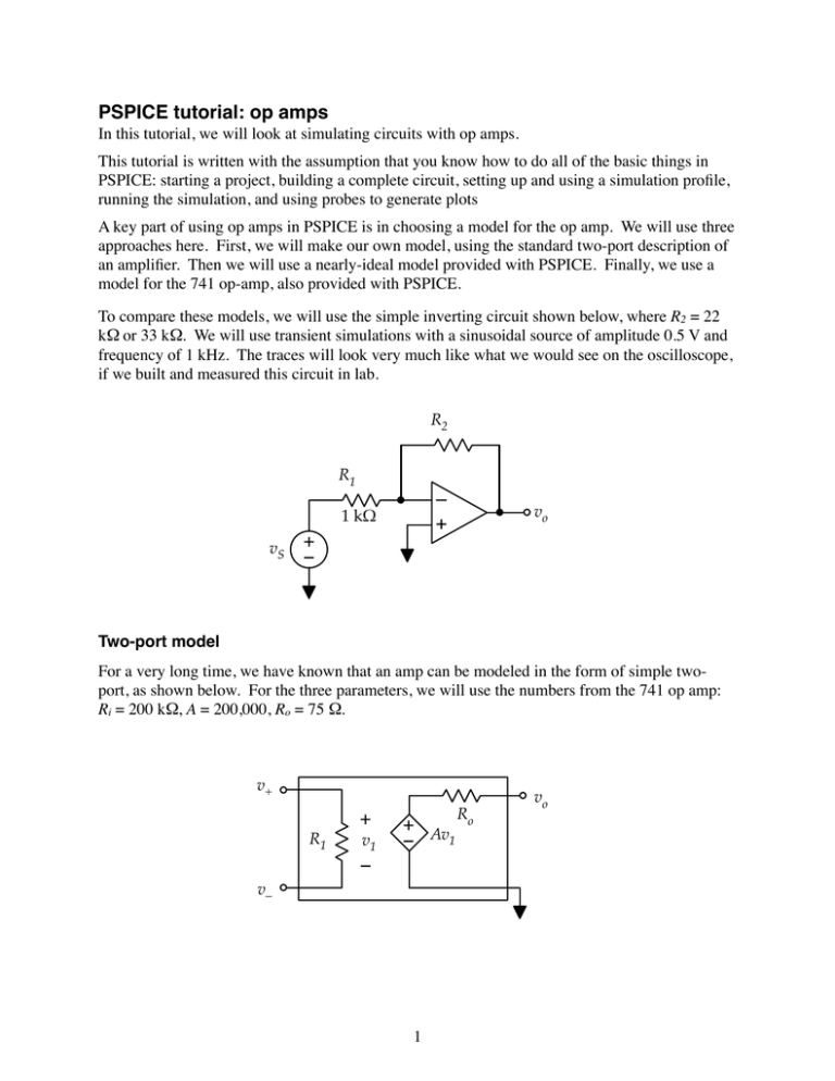
PSPICE tutorial: op amps In this tutorial, we will look at simulating circuits with op amps. This tutorial is written with the assumption that you know how to do all of the basic things in PSPICE: starting a project, building a complete circuit, setting up and using a simulation profile, running the simulation, and using probes to generate plots A key part of using op amps in PSPICE is in choosing a model for the op amp. We will use three approaches here. First, we will make our own model, using the standard two-port description of an amplifier. Then we will use a nearly-ideal model provided with PSPICE. Finally, we use a model for the 741 op-amp, also provided with PSPICE. To compare these models, we will use the simple inverting circuit shown below, where R2 = 22 kΩ or 33 kΩ. We will use transient simulations with a sinusoidal source of amplitude 0.5 V and frequency of 1 kHz. The traces will look very much like what we would see on the oscilloscope, if we built and measured this circuit in lab. ! ! ! ! ! ! ! ! ! ! ! R2 R1 – + 1 k! vS + – vo Two-port model For a very long time, we have known that an amp can be modeled in the form of simple twoport, as shown below. For the three parameters, we will use the numbers from the 741 op amp: Ri = 200 kΩ, A = 200,000, Ro = 75 Ω. ! ! ! ! ! ! ! ! ! v+ + R1 v1 + Av 1 – – v– 1 Ro vo Using the two-port model to implement the feedback circuit in PSPICE leads to the circuit shown below. (If it looks a bit odd, it’s because it is “upside-down” from the usual way we draw an inverting op-amp circuit.) Obviously, we expect the gain to be -22. The simulation is set up to run for 5 ms (5 periods of the sinusoid) with a maximum step size of 0.01 ms, giving at least 500 points in the simulation. ! ! ! ! ! ! ! ! ! ! The input and output traces from the simulation are shown below. The traces match expectations almost exactly. ! ! 2 If R2 is increased to 33 kΩ, the gain increase accordingly. The input and output traces in that case are shown below. Again, there are no surprises. The two-port model describes the basic behavior of an ideal op amp very well. As we discussed in class, the feedback makes the exact values of Ri, A, and Ro somewhat irrelevant. As long as the gain is big enough, the amp will operate in a nearly ideal fashion. The two-port model does not include any means to exhibit non-ideal effects of offset voltage/bias currents, output-voltage clipping, slew-rate limits, gain-bandwidth limits, or output-current limitations. These could be added, but the circuit model will become much more complicated. ! ! 3 (Nearly) ideal op amp from PSPICE Next lay out the circuit shown below. Use the OPAMP model from the Analog library. This appears to a be an ideal op amp model. (When you first place the symbol in the drawing window, the non-inverting terminal is on top. If you select the amp, and then right-click on it, you can choose the “Mirror vertically” option from the pop-up menu. The “flips the amp over” so that the inverting terminal is on top, and then you can wire up the inverting circuit in the “normal” fashion.) Note the the in the figure below, R2 = 33 kΩ. However, you should start with R2 = 22 kΩ. ! ! ! ! ! ! ! ! ! ! ! Then, running the transient simulation, with R2 = 22 kΩ gives the expected results, shown below. 4 However, if we increase R2 to 33 kΩ, we learn that the OPAMP part is not really ideal. In trying to run the simulation, we encounter a continuous string of computation errors. Eventually, we give up and assume that that we are doing something wrong. Playing around a bit, we note that for any value of R2 less than 29 kΩ, the simulation will run with no problems, but fails miserable for resistance above that value. There might be a clue in this: At R2 = 29 kΩ, the expected peak value of the output would be 14.5 V. Playing around a bit more, if we select the OPAMP part and then right-click on it, we note that among the available menu items is one called “Edit properties…”. Choosing that one presents us with a new window that has pair of long horizontal rows of cells. (It looks a bit like two rows from an Excel file – a title row and a data row.) Most of the information the cells is indecipherable (at least to us right now), but if we scroll horizontally we see a couple of familiar things. First, we find a Gain entry, with a value of 106. So evidently, the gain in the OPAMP model is one million. Then if scroll clear to the right end of the double row of cells, we find entries for VNEG (= –15 V) and VPOS (= +15 V). ! Aha! So apparently the OPAMP model is not ideal – it appears to imposing some sort of powersupply-like limit on the output. However, it seems to do it in a very clumsy fashion – by causing the simulation itself to fail, rather than actually clipping the output voltage. The values for VNEG and VPOS can be altered. If we change them to something larger (say ± 25 V), we might be might be able to run the simulation with a higher gain. So we change the values and close the Property Editor window. Then, re-running the simulation with the new VNEG and VPOS properties and with R2 = 22 kΩ gives a more satisfying result, shown at the top of the next. Commentary: We have no idea what sort of mathematical description is being used to control the behavior of the OPAMP model. We are completely at the mercy of whoever put that model together. Without having more detailed knowledge of the internal mathematical description of the model, we should be cautious in using it. OPAMP appears to be an almost ideal op amp and will probably work OK for many simulations, but there may be other non-idealities lurking inside. 5 Input and output voltage traces for the inverting amp with R2 = 33 kΩ and VNEG/VPOS changed to ±25 V ! The uA741 op amp model! Finally, let’s use a model that purports to represent a real part. The uA741 model is located in the EVAL library. (So you will have to add EVAL to your list of libraries in PSPICE.) The uA741 is the very last entry in that library. The model has lots of connections – the usual three (v+, v_, and vo), two power supplies, and two for the offset voltage correction feature of the 741. Obviously, we need to use v+, v_, and vo. We also need to connect DC power supplies. The leads for the offset voltage correction can be left unconnected, just as we did when we used the 741 in lab. Wiring up the inverting amp with the uA741 model, we have the circuit diagram shown below. ! ! ! ! ! ! 6 Running the transient simulation with R2 = 22 kΩ gives us (once again) the expected output. Changing R2 to 33 kΩ and re-running the simulation shows us that the uA741 model does incorporate power supply clipping in its mathematical description. So it looks like the uA741 model has the potential to be a reasonably accurate PSPICE op amp description. However, unless we tear into the internals of the mathematical description or do some experimentation, we don’t know how the model handles other non-ideal effects, like slew rate, gain-bandwidth, etc. So again, we should use this model with caution. 7


