PCB Layout Guidelines for Power Controllers
advertisement
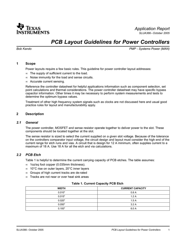
Application Report SLUA366 – October 2005 PCB Layout Guidelines for Power Controllers Bob Kando .............................................................................................. PMP - Systems Power (MAN) 1 Scope Power layouts require a few basic rules. This guideline for power controller layout addresses: • The supply of sufficient current to the load. • Noise immunity for the load and sense circuits. • Accurate current sensing. Reference the controller datasheet for helpful applications information such as component selection, set point calculations and thermal considerations. The power controller datasheet may have specific bypass capacitor information. Other times it may be necessary to perform system measurements and tests to determine the optimum bypass values. Treatment of other high frequency system signals such as clocks are not discussed here and usual good practice rules for layout and manufacturability apply. 2 Description 2.1 General The power controller, MOSFET and sense resistor operate together to deliver power to the slot. These components should be located together at the slot. The sense resistor is sized to select the current supplied on a given slot voltage. Because of the tolerance on the controllers comparator input voltage, the circuit design and layout must consider the high end of the current range for etch runs and vias. A circuit that is design for 12 A minimum, often supplies current to a maximum of 18 A. Use 18 A for all the etch and via calculations. 2.2 PCB Etch Table 1 is helpful to determine the current carrying capacity of PCB etches. The table assumes: • 1oz/sq foot copper (0.035mm thickness). • 10°C rise on outer layers, 20°C inner layers • Groups of high current tracks are de-rated • Tracks are not near or over heat sink areas Table 1. Current Capacity PCB Etch SLUA366 – October 2005 WIDTH CURRENT CAPACITY 0.010" 0.8 A 0.015" 1.2 A 0.020" 1.5 A 0.050" 3.2 A 0.100" 6.0 A PCB Layout Guidelines for Power Controllers 1 www.ti.com Description From Table 1, each doubling of copper thickness allows an increase of sqrt(2) (about 1.4) in the current capacity. Each doubling of a single track width increases current capacity by a factor of 1.65. For our 12-A minimum output example, the etch run should be designed for 18 A. Using 1 ounce copper, an etch width of 0.35 inches is minimum for a 10°C rise on the outer layers. 2.3 Vias or Feedthrus Vias limit the current and add inductance between the power supply and load. Layouts are usually done with 10-mil inner ring feedthrus. At this size, current capability is about 1 A per feedthru. To access power from the inner layer plane to the MOSFET input in our example requires 18 feedthrus Bypass capacitors should be located on the same side of the board as the target component as close to the component as possible. If feedthrus are used, the design must consider the inductance of the feedthru. It may require multiple feedthrus just to reduce the inductance. Multiple capacitors may be required for bulk or low or high frequency filtering. At higher operating frequencies, the inductance is a more sever problem. Bypassing a 100-MHz signal is extremely difficult with feedthrus in the circuit. High frequency bypassing is best done on the component plane with no vias. 2.4 Sense Resistor Wiring The sense resistor is as much as possible a direct connection between the MOSFET output and the slot power. Similar to the MOSFET circuits, the sense resistor etch must be sized to the maximum current requirement. The sense etch should be connect between the resistor bond pads and run as a differential pair to the hot plug controller. In this way, the sense voltage is measured directly across the sense resistor and is not influenced by other circuit board etch. The Kelvin connection is shown in Figure 1. Accuracy of the sense resistor measurement will be compromised if these details are not met. Figure 1. Kelvin Connection 2 PCB Layout Guidelines for Power Controllers SLUA366 – October 2005 www.ti.com Description 2.5 Sense Resistor Bypass Power circuits often have high current transients. These transients can cause voltage spikes across the sense resistors that can trip the hot plug controller. Bypassing across the sense resistor inputs to the hot plug controller may be required. A 1-nF capacitor located at the controller on the sense resistor input pins is usually sufficient to filter noise above 1 MHz. The capacitor value is selected based on the Impedance vs Frequency graph, Figure 2. Other filtering schemes may be necessary. Common mode noise may be better addressed with capacitors on each side of the sense resistor to ground. Adequate bypassing of the power to the FET and to the load is very important because the sense resistor and FET should not see high frequency current fluctuations. IMPEDANCE vs FREQUENCY 1000 0.001µF 100 Impedance − Ω 0.01µF 10 0.1µF 1.0 0.1 10µF 0.01 10K 100K 1M 10M 100M 1G f − Frequency − Figure 2. 2.6 Supply Bypass Ground noise can be a major problem on backplanes with high current switching. The switching current from the PCIX and PCIX-2 transceivers with an all 1’s pattern to all 0’s can be 3.2 A per slot from the transceivers alone. The logic adds additional noise which can be measured across the ground plane and slot power. The noise may be coupled into sense lines or other signals through bypass capacitors not grounded close to the part that they are bypassing. SLUA366 – October 2005 PCB Layout Guidelines for Power Controllers 3 www.ti.com Description 2.7 Bulk Capacitance A bulk capacitor adds stability to the power supply voltage because it can supply surge current to the load. Adequate bulk capacitance for the input supply voltage should be located at the MOSFET input. Sense resistor output voltage to the slot should have bulk capacitance and high frequency bypass located at the slot. Bulk capacitance can be calculated by C = I x ∆t / ∆V; where I is the surge current, ∆V is the voltage drop that can be tolerated, and ∆t is the duration of the surge. To Load To Power Supply BULK 10 nF BULK VCC GATE 10 nF RS 1 nF RS To Inner Layer Power Bulk D S S D MOSFET S D G D Vcc 10nF Gnd 1nF Controller Sense Resistor Load Connection Figure 3. Sample Schematic and Layout 2.8 Summary Providing the correct etch width, number of vias and adequate bypassing will reduce the debug time and speed the time to market. Noise and supply problems generate random errors that are often hard to track down, which take a lot of time. Following a basic set of power rules will reduce test time and time to market. 4 PCB Layout Guidelines for Power Controllers SLUA366 – October 2005 IMPORTANT NOTICE Texas Instruments Incorporated and its subsidiaries (TI) reserve the right to make corrections, modifications, enhancements, improvements, and other changes to its products and services at any time and to discontinue any product or service without notice. Customers should obtain the latest relevant information before placing orders and should verify that such information is current and complete. All products are sold subject to TI’s terms and conditions of sale supplied at the time of order acknowledgment. TI warrants performance of its hardware products to the specifications applicable at the time of sale in accordance with TI’s standard warranty. Testing and other quality control techniques are used to the extent TI deems necessary to support this warranty. Except where mandated by government requirements, testing of all parameters of each product is not necessarily performed. TI assumes no liability for applications assistance or customer product design. Customers are responsible for their products and applications using TI components. To minimize the risks associated with customer products and applications, customers should provide adequate design and operating safeguards. TI does not warrant or represent that any license, either express or implied, is granted under any TI patent right, copyright, mask work right, or other TI intellectual property right relating to any combination, machine, or process in which TI products or services are used. Information published by TI regarding third-party products or services does not constitute a license from TI to use such products or services or a warranty or endorsement thereof. Use of such information may require a license from a third party under the patents or other intellectual property of the third party, or a license from TI under the patents or other intellectual property of TI. Reproduction of information in TI data books or data sheets is permissible only if reproduction is without alteration and is accompanied by all associated warranties, conditions, limitations, and notices. Reproduction of this information with alteration is an unfair and deceptive business practice. TI is not responsible or liable for such altered documentation. Resale of TI products or services with statements different from or beyond the parameters stated by TI for that product or service voids all express and any implied warranties for the associated TI product or service and is an unfair and deceptive business practice. TI is not responsible or liable for any such statements. Following are URLs where you can obtain information on other Texas Instruments products and application solutions: Products Applications Amplifiers amplifier.ti.com Audio www.ti.com/audio Data Converters dataconverter.ti.com Automotive www.ti.com/automotive DSP dsp.ti.com Broadband www.ti.com/broadband Interface interface.ti.com Digital Control www.ti.com/digitalcontrol Logic logic.ti.com Military www.ti.com/military Power Mgmt power.ti.com Optical Networking www.ti.com/opticalnetwork Microcontrollers microcontroller.ti.com Security www.ti.com/security Telephony www.ti.com/telephony Video & Imaging www.ti.com/video Wireless www.ti.com/wireless Mailing Address: Texas Instruments Post Office Box 655303 Dallas, Texas 75265 Copyright 2005, Texas Instruments Incorporated
