Introducing a 3 x 3 mm QFN Style Fully Integrated Linear Sensor IC
advertisement
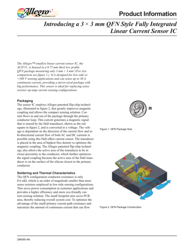
Product Information Introducing a 3 × 3 mm QFN Style Fully Integrated Linear Current Sensor IC The Allegro™ smallest linear current sensor IC, the ACS711, is housed in a 0.75 mm thick low profile QFN package measuring only 3 mm × 3 mm! (For size comparison see figure 1.) It is designed for low-side or <100 V sensing applications and can sense up to 30 A continuous current, providing a micro-sized package with big performance. This sensor is ideal for replacing sense resistor op-amp current sensing configurations. Packaging The sensor IC employs Allegro patented flip-chip technology, illustrated in figure 2, that greatly improves magnetic coupling and allows the compact sensing solution. Current flows in and out of the package through the primary conductor loop. This current generates a magnetic signal that is sensed by the Hall transducer, shown as the red square in figure 2, and is converted to a voltage. The voltage is dependent on the direction of the current flow and so bi-directional current flow of both AC and DC currents is possible using this Hall effect current sensor. The transducer is placed in the area of highest flux density to optimize the magnetic coupling. The Allegro patented flip-chip technology also allows the active area of the transducer to be in closer proximity to the conductor, which further optimizes the signal coupling because the active area of the Hall transducer is on the surface of the silicon closest to the primary conductor. Soldering and Thermal Characteristics The QFN configuration conductor resistance is only 0.6 mΩ, which is an order of magnitude smaller than most sense resistors employed in low-side sensing configurations. This saves power consumption in customer applications and provides a higher efficiency and more eco-friendly current sensing solution. The small footprint also saves PCB area, thereby reducing overall system cost. To optimize the advantage of the small primary current path resistance and maximize the amount of continuous current that can flow 296095-AN Figure 1. QFN Package Size Figure 2. QFN Package Construction through the Allegro package, conducting heat away from the device must be considered. Figure 3 illustrates an optimized PCB layout for the QFN package. For peak thermal and electrical performance, the following features should be included in the PCB layout: • Primary current leads should be connected to as much surface area of copper as is reasonably available. The two solder pads at the ends of the exposed pad loop should be placed directly on the current carrying copper trace to best conduct heat away from the package, and is clearly illustrated in figure 3. • The copper thickness should be 4 oz. Using 2 oz. copper will reduce performance. • If possible, additional copper layers, or at least two layers, should be used for conducting the primary current. The layers should be connected using the arrangement of vias shown in figure 3 and placed close to the primary current leads of the QFN package. • Vias under the exposed QFN pads are excellent for conducting heat away from the package, but these vias must be plugged in order to prevent wicking of the solder from the pad into the via during reflow. Care must be taken when using these types of vias and size, quantity, and placement should be considered based on the application. By applying these features, it is possible to achieve the thermal performance shown in figure 4. The data was taken using a test demonstration board with a solder footprint similar to the one shown in figure 3, and using two layers of 4 oz. copper. The graph shows that at an ambient temperature of 85°C the sensor package can withstand 45 A continuous current before reaching the maximum recommended thermal junction (die) temperature of 165°C. With proper PCB design, the device can be safely used in 30 A continuous current applications up to 85°C ambient temperature with greater than 40°C of safety margin before reaching a die temperature of 165°C. Figure 3. PCB Layout for QFN Current Sensor 296095-AN Allegro MicroSystems, LLC 115 Northeast Cutoff Worcester, Massachusetts 01615-0036 U.S.A. 1.508.853.5000; www.allegromicro.com 2 Device Accuracy and Fault Output Sense resistor op-amp solutions suffer accuracy error as the sense resistor changes with temperature. Since the magnetic field generated by current flowing in a conductor is not temperature dependent, Hall sensors are not subject to this error term. In addition, the fully integrated architecture of the ACS711 sensor IC allows the major error terms, both gain and offset, to be programmed at end-of-line production to produce a more accurate Hall-effect current sensing solution that is easy for designers to employ in the application. The ACS711 sensor IC also integrates a factory-programmed fast response digital fault output that has a 1.3 μs response time. This fast fault can be used to prevent the destruction of IGBTs or other switching devices during short circuit or overcurrent conditions, or as a redundant fault feature in motor control applications. Summary Advanced Allegro patented flip-chip packaging for linear Hall ICs has allowed the creation of a micro-sized, 3 mm × 3 mm fully integrated current sensor device, the Allegro MicroSystems ACS711, which has only a 0.6 mΩ internal resistance, produced in a package that can really take the heat. Used with an appropriate PCB design, the device can be used for applications with over 30 A continuous current while reducing power consumption by an order of magnitude in comparison with existing sense resistor op-amp solutions. Factory programming provides high accuracy in this IC, with an integrated fast response fault output. Together these techniques deliver the smallest current sensing footprint available for your application without compromising accuracy. ACS711 Die Temperature versus Continuous Current 180 °C 5°C = 125 =8 ature r e e r p m tu °C nt Te era 25 Ambie = mp e e T r nt tu ra bie pe Am m Te t n bie Am Die Temperature, TJ, (°C) 160 140 120 100 80 60 40 20 0 0 10 20 30 40 50 60 Continuous Current (DC) (A) Figure 4. QFN Current Sensor Linear Thermal Performance on PCB 296095-AN Allegro MicroSystems, LLC 115 Northeast Cutoff Worcester, Massachusetts 01615-0036 U.S.A. 1.508.853.5000; www.allegromicro.com 3 Based on an article originally published in Electronics, Datastream Business Media Limited, September 2012. For portions not copyrighted by original publisher, Copyright ©2012-2013, Allegro MicroSystems, LLC The information contained in this document does not constitute any representation, warranty, assurance, guaranty, or inducement by Allegro to the customer with respect to the subject matter of this document. The information being provided does not guarantee that a process based on this information will be reliable, or that Allegro has explored all of the possible failure modes. It is the customer’s responsibility to do sufficient qualification testing of the final product to insure that it is reliable and meets all design requirements. For the latest version of this document, visit our website: www.allegromicro.com 296095-AN Allegro MicroSystems, LLC 115 Northeast Cutoff Worcester, Massachusetts 01615-0036 U.S.A. 1.508.853.5000; www.allegromicro.com 4
