Lsupp - PopLab@Stanford
advertisement
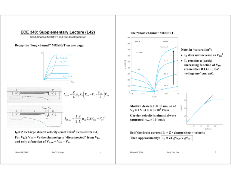
ECE 340: Supplementary Lecture (L42) The “short channel” MOSFET. Short-Channel MOSFET and Non-Ideal Behavior Recap the “long channel” MOSFET on one page: Note, in “saturation”: • ID does not increase as VGS2 • ID remains a (weak) increasing function of VDS (remember B.I.G…. mo’ voltage mo’ current). I D ,lin = V Z μeff Ci VGS − VT − DS VDS L 2 Modern devices L ≈ 35 nm, so at VD ≈ 1 V E ≈ 3×10⁵ V/cm I D , sat = 1Z μeff Ci (VGS − VT ) 2 2L Carrier velocity is almost always saturated! vsat ≈ 107 cm/s ID ≈ Z × charge sheet × velocity (cm × C/cm2 × cm/s = C/s = A) So if the drain current ID ≈ Z × charge sheet × velocity For VD ≥ VGS – VT the channel gets “disconnected” from VD, and only a function of VD,sat = VGS – VT. Then approximately: ID ≈ ZCi(VGS-VT)vsat Illinois ECE340 Prof. Eric Pop 1 Illinois ECE340 Prof. Eric Pop 2 Last result is a bit counterintuitive, but pretty important! ΔL = λ (VDS − VDSsat ) L • ID,sat proportional to (VGS – VT) rather than (VGS – VT)2 • ID,sat is practically independent of L! I 'D , sat = I D , sat [1 + λ (VDS − VDSsat )] • So to get more current, scale VT and/or Ci instead of L Luckily, we do get one break as devices get smaller = velocity overshoot: What if I keep increasing VD and/or decreasing L? • For very short L (~ 10–50 nm) some electrons travel across the channel without ___scattering_____ • Those “ballistic” electrons can achieve v > vsat • This effectively raises the collective vsat > 107 cm/s (~30% increase for 100 nm NFET, more if shorter) What about the weak dependence of ID,sat on VDS? Avalanche (impact ionization) This is due to “channel length modulation” L’ = L – ΔL Where ΔL α (VDS – VDS,sat) Illinois ECE340 Prof. Eric Pop 3 Illinois ECE340 Prof. Eric Pop 4 A note on sub-threshold behavior. So far, we’ve assumed no channel current (ID=0) if VGS < VT. This is incorrect. Transistor constant-field scaling (Dennard’s Law) If ϕS > ϕF, there is some (weak) inversion charge at the surface, which gives rise to sub-threshold current flowing between the source and drain: 2 kT q (VG −VT )/ mkT Z (1 − e − qVDS / kT ) I D = μeff Cox (m − 1) e L q Where m is ___________________. Note exponential dependence on voltages, suggesting ID below threshold is in fact limited by __________________. Define sub-threshold slope, S: −1 d (log10 I D ) C kT = S ≡ ln (10)(1 + d ) q Cox dVGS VT design trade-off: • High ON current ID α (VDS – VT)n requires ________ VT • Low OFF current requires _________ VT Typical value: 70–100 mV/decade. Want it small! (why?) log IDS Low VT High VT IOFF,low VT IOFF,high VT 0 Illinois ECE340 Prof. Eric Pop 5 Illinois ECE340 Prof. Eric Pop VGS 6 Since VT cannot be scaled down aggressively, the powersupply voltage (VDD = max VDS) has not been scaled down in proportion to the MOSFET dimensions: Today (if using SiO2 gate oxide): ~35-45 nm ~1-1.25 V 10-20 Å 5 MV/cm …with HfO2 gate oxide: _______ ________ Illinois ECE340 Prof. Eric Pop 7 ECE 340: Supplementary Lecture (L43) MOSFET Scaling Limits 3) Variability in circuit printing (lithography) as features are well below the light wavelength used. Some modern CMOS limitations: Intended Layout Layout 1) Power and leakage were shown in L42. 2) Memory is often a speed bottleneck. So modern CPUs are full of on-chip cache, which occupies 50% or more of floor space, leaving less room for logic. Why? An SRAM cell is BIG (six transistors), area ~ 20x7 = 140F2 where F is the transistor technology node (e.g. 65 nm). 0.13µ 0.25µ 0.18µ 90-nm 65-nm Gates Source/Drain regions (p-type wider than n-type) Intended Layout at 90 nm without optical correction Note: Invention of electrically accessible (preferably non-volatile) memory with high speed and high density would lead to a revolution in computer architectures. with optical correction Illinois ECE340 Prof. Eric Pop 1 Illinois ECE340 Prof. Eric Pop 2 4) Variability in gate oxide thickness (moving to HfO2 helps, as it gives us more room for atomic-layer error) 5) Variability in dopant atom numbers Well-behaved MOSFET we want Illinois ECE340 A 22 nm MOSFET only has 50 silicon atoms along channel surface, and about just as many dopant atoms (red) in the source/drain regions. Prof. Eric Pop A 4 nm MOSFET would only have 10 silicon atoms along the channel surface. 3
