Week 2 Discussion Notes
advertisement
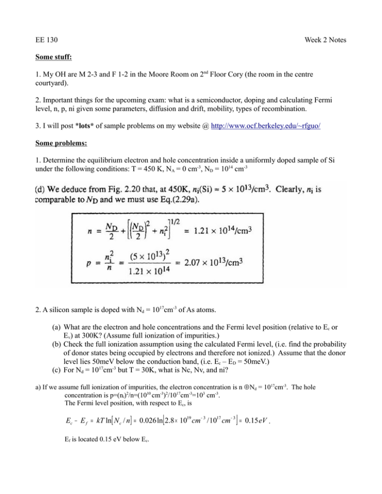
EE 130 Week 2 Notes Some stuff: 1. My OH are M 2-3 and F 1-2 in the Moore Room on 2nd Floor Cory (the room in the centre courtyard). 2. Important things for the upcoming exam: what is a semiconductor, doping and calculating Fermi level, n, p, ni given some parameters, diffusion and drift, mobility, types of recombination. 3. I will post *lots* of sample problems on my website @ http://www.ocf.berkeley.edu/~rfguo/ Some problems: 1. Determine the equilibrium electron and hole concentration inside a uniformly doped sample of Si under the following conditions: T = 450 K, NA = 0 cm-3, ND = 1014 cm-3 2. A silicon sample is doped with Nd = 1017cm-3 of As atoms. (a) What are the electron and hole concentrations and the Fermi level position (relative to Ec or Ev) at 300K? (Assume full ionization of impurities.) (b) Check the full ionization assumption using the calculated Fermi level, (i.e. find the probability of donor states being occupied by electrons and therefore not ionized.) Assume that the donor level lies 50meV below the conduction band, (i.e. Ec – ED = 50meV.) (c) For Nd = 1017cm-3 but T = 30K, what is Nc, Nv, and ni? a) If we assume full ionization of impurities, the electron concentration is n ≈ Nd = 1017cm-3. The hole concentration is p=(ni)2/n=(1010 cm-3)2/1017cm-3=103 cm-3. The Fermi level position, with respect to Ec, is [ ] Ec − E f = kT ln[ N c / n] = 0.026 ln 2.8 × 1019 cm− 3 / 1017 cm − 3 = 0.15 eV . Ef is located 0.15 eV below Ec. b) In order to check the full ionization assumption with the calculated Fermi level, we need to find the percentage of donors occupied by electrons. ED − E f = ( Ec − E f ) − ( Ec − ED ) = 0.1eV , and nD = N d 1 1+ e ( E D − E f ) / kT = ( ) 1017 cm − 3 15 −3 ( 0.1 eV / 0.026 eV ) = 2.09 × 10 cm ≡ 2% of N d . 1+ e Since only 2% of dopants are not ionized, it is fine to assume that the impurities are fully ionized. c) For T=30 K, we need to use Equation (1.10.2) to find the electron concentration since the temperature is extremely low. First, we calculate Nc and Nv at T = 30 K: 3/ 2 2 mdn kT 3/ 2 T 19 N C T =30 K =2[ ] =3.217×10 × cm−3=1.0173×1018 cm−3 and 2 300 K h 3/2 2 mdp kT T 3 / 2 −3 19 N v T =30 K =2[ ] =1.83×10 × cm =5.787×1017 cm−3 2 300 K h ni = N c ( 30 K ) N v ( 30 K ) − ( E g ) / ( 2 kT ) e = 2.32 × 10 − 75 cm − 3 . 2 3. a) Consider a Si sample maintained at room temp under equilibrium conditions doped with phosphorus to a concentration of 10^16 cm^-3. i. What are the electron and hole concentrations (n and p) in this sample? Is the material ntype or p-type? ii. Draw the energy band diagram for this sample. b) Suppose the sample is counterdoped to the opposite type by boron s.t. Ei – EF = 0.30 eV. i. What are n and p in the counter-doped sample? ii. What is the concentration of boron? (a) i. Phosphorus atoms are donors (Nd). Therefore, the sample is n-type with an electron concentration equal to Nd = 1x1016 cm-3 (since it is appropriate to assume full-ionization at room temperature). Thus: n = Nd = 1x1016 cm-3 p = (ni)2/n = (1x1010 cm-3)2/1x1016 cm-3 = 1 x104 cm-3 (b) ii. E F −E i=kT ln [ b) i. 300 meV below Ei. n ~ 10^5 cm^-3 n ]=6kT ln10=0.360 eV 0.360 eV above Ei ni p=ni e E −E i F / kT =1×10¹⁰×e 0.3/0.0259 =1.03×10 15 cm−3 By charge neutrality equation: p – n + N_d+ - N_A- = 0 N_A- = p + N_D+ = 1.1 x 10^16 cm^-3 of Boron 4. A p-type (uncompensated) silicon sample is maintained at 300K. When an electric field with strength 5×10³ V/cm is applied to the sample, the electron drift velocity is 4×106 cm/sec. a) What is the mean free path of an electron in this sample? (Note: 1 kg cm2/V/s/C = 10-4 sec) b) What is the resistivity of this sample? a) Find µn and τmp: v d 4 × 10 6 cm / s = ε 5 × 10 3 V / cm = 800 cm 2 V − 1 s − 1 µn = τ mn = mn* µ q n = 0.26 ⋅ 9.11 × 10 − 31 kg ⋅ 800 cm 2 V − 1 s − 1 × 10 − 4 s − 19 1.6 × 10 coul = 1.18 × 10 − 13 s = 0.118 ps Use vth and τmn to find l: l = vthτ mn = 2.30 × 10 7 cm / s ⋅ 0.118 ps = 2.71 × 10 − 6 cm = 27.1 nm b) To find resistivity, we need to know the dopant concentration NA. Using Figure 3.5 (mobility vs. total dopant concentration) on Page 80 of Pierret, we find that for an electron mobility of 800 cm2V-1s-1, NA + ND = 1017 cm-3 and the hole mobility is ~330 cm2V-1s-1. Since the sample is uncompensated, ND = 0 so NA = 1017 cm-3. ρ = 1 qpµ = p 1.6 × 10 − 19 1 C ⋅ 10 cm − 3 ⋅ 330 cm 2V − 1 s − 1 17 = 0.19 Ω − cm 5. A sample of N-type silicon is at room temperature. When an electric field with strength of 1000V/cm is applied to the sample, the hole velocity is measured and found to be 2x105 cm/sec. (a) Estimate the thermal equilibrium electron and hole densities, indicating which is the minority carrier. (b) Find the position of Ef with respect to Ec and Ev. The sample is used to make an integrated circuit resistor. The width and height of the sample are 10µm and 1.5µm, respectively, and the length of the sample is 20µm. Calculate the resistance of the sample. It is given that the sample is n-type, and the applied electric field ε is1000V/cm. The hole velocity υdp is 2×105cm/s. (a) From the velocity and the applied electric field, we can calculate the mobility of holes: υdp = µpε, µp = υdp/ε = 2×10⁵/1000 = 200cm2/V·s. From Fig. 3.5 a), we find Nd is equal to 4.5×10¹⁷/cm3. Hence, n = Nd = 4.5×10¹⁷/cm3, and p = ni2/n = ni2/ Nd = 1020 / 4.5×1017 = 222/cm3. Clearly, the minority carrier is hole. (b) The Fermi level with respect to Ec is Ef = Ec - kTln(Nd/Nc) = Ec - 0.107 eV. (c) R = ρL/A. Using Equation (2.2.14), we first calculate the resistivity of the sample: σ = q(µn n + µp p) ≈ qµn n = 1.6×10-19 × 400 × 4.5×1017 = 28.8/Ω-cm, and ρ= σ -1 = 0.035 Ω-cm. Therefore, R = (0.035) × 20µm / (10µm× 1.5µm) = 467 Ω.
