Deliverable 1.8a: Circuit tapeout #1
advertisement

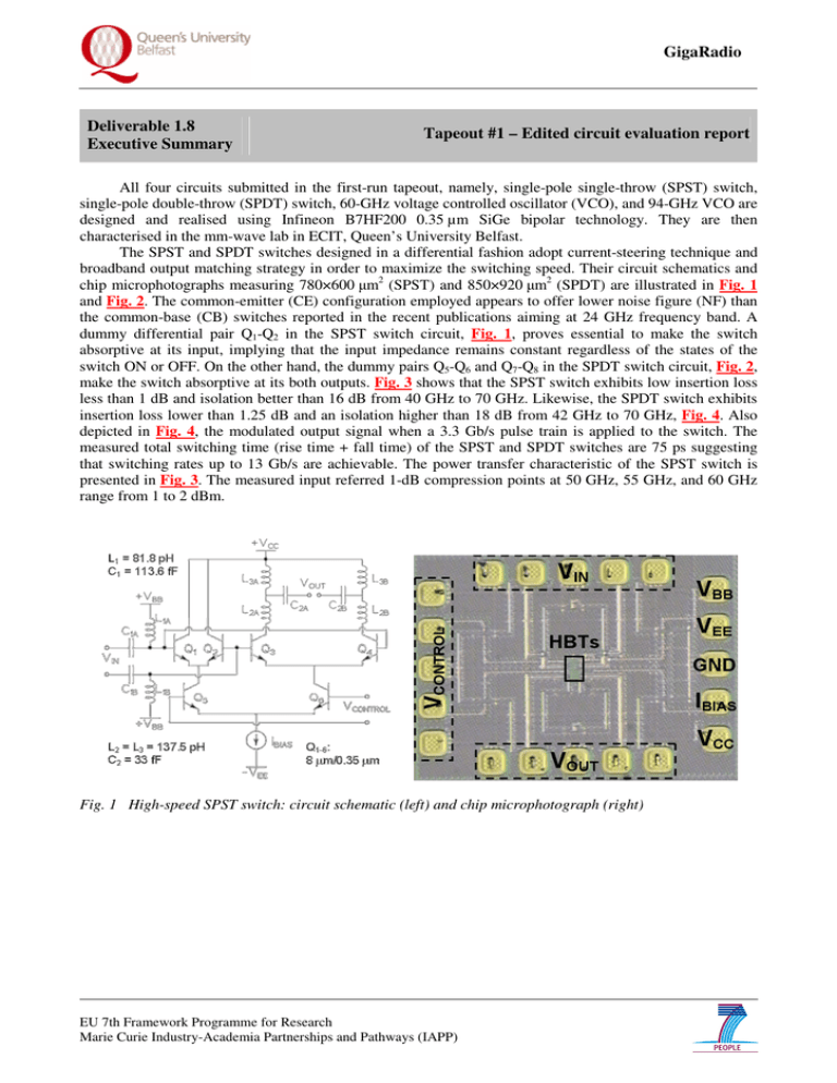
GigaRadio Deliverable 1.8 Executive Summary Tapeout #1 – Edited circuit evaluation report All four circuits submitted in the first-run tapeout, namely, single-pole single-throw (SPST) switch, single-pole double-throw (SPDT) switch, 60-GHz voltage controlled oscillator (VCO), and 94-GHz VCO are designed and realised using Infineon B7HF200 0.35 µm SiGe bipolar technology. They are then characterised in the mm-wave lab in ECIT, Queen’s University Belfast. The SPST and SPDT switches designed in a differential fashion adopt current-steering technique and broadband output matching strategy in order to maximize the switching speed. Their circuit schematics and chip microphotographs measuring 780×600 µm2 (SPST) and 850×920 µm2 (SPDT) are illustrated in Fig. 1 and Fig. 2. The common-emitter (CE) configuration employed appears to offer lower noise figure (NF) than the common-base (CB) switches reported in the recent publications aiming at 24 GHz frequency band. A dummy differential pair Q1-Q2 in the SPST switch circuit, Fig. 1, proves essential to make the switch absorptive at its input, implying that the input impedance remains constant regardless of the states of the switch ON or OFF. On the other hand, the dummy pairs Q5-Q6 and Q7-Q8 in the SPDT switch circuit, Fig. 2, make the switch absorptive at its both outputs. Fig. 3 shows that the SPST switch exhibits low insertion loss less than 1 dB and isolation better than 16 dB from 40 GHz to 70 GHz. Likewise, the SPDT switch exhibits insertion loss lower than 1.25 dB and an isolation higher than 18 dB from 42 GHz to 70 GHz, Fig. 4. Also depicted in Fig. 4, the modulated output signal when a 3.3 Gb/s pulse train is applied to the switch. The measured total switching time (rise time + fall time) of the SPST and SPDT switches are 75 ps suggesting that switching rates up to 13 Gb/s are achievable. The power transfer characteristic of the SPST switch is presented in Fig. 3. The measured input referred 1-dB compression points at 50 GHz, 55 GHz, and 60 GHz range from 1 to 2 dBm. Fig. 1 High-speed SPST switch: circuit schematic (left) and chip microphotograph (right) EU 7th Framework Programme for Research Marie Curie Industry-Academia Partnerships and Pathways (IAPP) GigaRadio Fig. 2 High-speed SPDT switch: circuit schematic (left) and chip microphotograph (right) Fig. 3 Measured results of the SPST switch: S-parameters (left) and power transfer (right) Fig. 4 Measured results of the SPDT switch: S-parameters (left) and modulated output signal with 3.3 Gb/s pulse train and 57 GHz carrier signal (right) EU 7th Framework Programme for Research Marie Curie Industry-Academia Partnerships and Pathways (IAPP) GigaRadio The circuit schematic of the 60-GHz VCO is illustrated in Fig. 5. It consists of a VCO core, a summing circuit, a single-ended to differential (STD) converter, and a buffer amplifier. The VCO core oscillates at half the desired frequency, i.e., 30 GHz and, by means of the summing circuit it is converted to the desired frequency, 60 GHz. On the other hand, the self-mixing 94-GHz VCO, depicted in Fig. 6, is comprised of a VCO core, a mixer, and an emitter coupled differential amplifier. The fundamental and second harmonic signals from the VCO core are supplied as LO and RF input signals for the mixer, respectively. The third harmonic of the mixing product is then amplified while the other unwanted harmonics are sufficiently suppressed. The chip microphotographs of the 60-GHz VCO measuring 900×550 µm2 and the 94-GHz VCO measuring 700×500 µm2 are presented in Fig. 7. The 60-GHz VCO operates from 58.85 GHz to 70.85 GHz with 20% frequency tuning range and the measured phase noise at 3-MHz offset plotted in Fig. 8 is less than -78 dBc/Hz across the entire tuning range. The measured gain is less than 1.6 GHz/V. The differential phase error of the output signals is measured by down converting the VCO output signals to low gigahertz frequency (around 3 GHz) using an on-chip mixer. The measured differential phase error is less than 8o. It consumes 70 mW under 3.5 V dc power supply. The 94-GHz VCO operates from 91 GHz to 101 GHz with 10.6% tuning range. The simulated harmonic suppression of the third harmonic relative to the fundamental is higher than 18 dB. The measured phase noise at 3 MHz offset, Fig. 8, is lower than -83 dBc/Hz over the entire frequency band. It consumes 185 mW under 3.5 V dc power supply. Fig. 5 Circuit schematic of the 60-GHz VCO Fig. 6 Circuit schematic of the 94-GHz VCO EU 7th Framework Programme for Research Marie Curie Industry-Academia Partnerships and Pathways (IAPP) GigaRadio Fig. 7 Chip microphotographs of the 60-GHz VCO (left) and 94-GHz VCO (right) Fig. 8 Measured phase noise at 3 MHz offset of the 60-GHz VCO (left) and 94-GHz VCO (right) EU 7th Framework Programme for Research Marie Curie Industry-Academia Partnerships and Pathways (IAPP)


