Design Tips: PCB Decoupling Capacitor Mounting Top – Bottom
advertisement
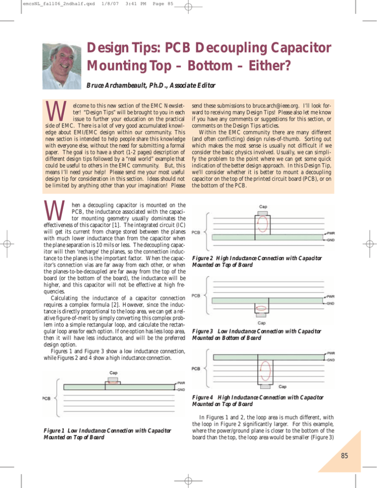
emcsNL_fall06_2ndhalf.qxd 1/8/07 3:41 PM Page 85 Design Tips: PCB Decoupling Capacitor Mounting Top – Bottom – Either? Bruce Archambeault, Ph.D., Associate Editor W elcome to this new section of the EMC Newsletter! “Design Tips” will be brought to you in each issue to further your education on the practical side of EMC. There is a lot of very good accumulated knowledge about EMI/EMC design within our community. This new section is intended to help people share this knowledge with everyone else, without the need for submitting a formal paper. The goal is to have a short (1-2 pages) description of different design tips followed by a “real world” example that could be useful to others in the EMC community. But, this means I’ll need your help! Please send me your most useful design tip for consideration in this section. Ideas should not be limited by anything other than your imagination! Please send these submissions to bruce.arch@ieee.org. I’ll look forward to receiving many Design Tips! Please also let me know if you have any comments or suggestions for this section, or comments on the Design Tips articles. Within the EMC community there are many different (and often conflicting) design rules-of-thumb. Sorting out which makes the most sense is usually not difficult if we consider the basic physics involved. Usually, we can simplify the problem to the point where we can get some quick indication of the better design approach. In this Design Tip, we’ll consider whether it is better to mount a decoupling capacitor on the top of the printed circuit board (PCB), or on the bottom of the PCB. W hen a decoupling capacitor is mounted on the PCB, the inductance associated with the capacitor mounting geometry usually dominates the effectiveness of this capacitor [1]. The integrated circuit (IC) will get its current from charge stored between the planes with much lower inductance than from the capacitor when the plane separation is 10 mils or less. The decoupling capacitor will then ‘recharge’ the planes, so the connection inductance to the planes is the important factor. When the capacitor’s connection vias are far away from each other, or when the planes-to-be-decoupled are far away from the top of the board (or the bottom of the board), the inductance will be higher, and this capacitor will not be effective at high frequencies. Calculating the inductance of a capacitor connection requires a complex formula [2]. However, since the inductance is directly proportional to the loop area, we can get a relative figure-of-merit by simply converting this complex problem into a simple rectangular loop, and calculate the rectangular loop area for each option. If one option has less loop area, then it will have less inductance, and will be the preferred design option. Figures 1 and Figure 3 show a low inductance connection, while Figures 2 and 4 show a high inductance connection. Figure 2 High Inductance Connection with Capacitor Mounted on Top of Board Figure 3 Low Inductance Connection with Capacitor Mounted on Bottom of Board Figure 4 High Inductance Connection with Capacitor Mounted on Top of Board Figure 1 Low Inductance Connection with Capacitor Mounted on Top of Board In Figures 1 and 2, the loop area is much different, with the loop in Figure 2 significantly larger. For this example, where the power/ground plane is closer to the bottom of the board than the top, the loop area would be smaller (Figure 3) 85 emcsNL_fall06_2ndhalf.qxd 1/8/07 3:41 PM Page 86 and the connection inductance would be lower if the capacitor were mounted on the back side of the board rather than the top side of the board. The opposite is true if the power/ground plane pair is near the top of the PCB, as shown in Figures 1 and 4. For an example, a large, ball grid array (BGA) device will have many power and ground pins. Often, decoupling capacitors are placed on the bottom side of the PCB across the BGA escape vias in order to minimize the connection inductance seen by the capacitor. If the power/ground plane pair in this example is close to the top of the PCB, then the rectangular loop between the capacitor and the planes would be smaller if the caps were placed on the top side of the board around the integrated circuit (IC). This type of analysis is also valid to decide if special board technologies, for example, buried capacitance, is worth the cost for your board stackup configuration. If the buried capacitance layer is deep in the board (closer to the bottom), then the rectangular loop area between the IC power/ground pins and the buried capacitance layer will be high, minimizing any good effects from the buried capacitance layer. Alternatively, if the buried capacitance layer is near the top of the PCB, the rectangular loop area is small, resulting in the IC receiving the benefit of the 86 buried capacitance layer without significant connection inductance. Summary There is no one correct answer to whether a decoupling capacitor should always be mounted on the top or bottom of a PCB. The best side of the PCB to mount the capacitor is the one where the rectangular loop area will be the smallest, resulting in the lowest inductance between the two options. References: [1] Wang, Chen, Jingkun Mao, Giuseppe Selli, Shaofeng Luan, Lin Zhang, Jun Fan, David J. Pommerenke, Richard E. DuBroff and James L. Drewniak, “An Efficient Approach for Power Delivery Network Design with Closed-Form Expressions for Parasitic Interconnect Inductance,” accepted for publication in IEEE Trans. on Advanced Packaging. [2] Knighten, J., B. Archambeault, J. Fan, G. Selli, L. Xue, S. Connor, J. Drewniak, “PDN Design Strategies: II. Ceramic SMT Decoupling Capacitors – Does Location Matter?” IEEE EMC Society Newsletter, Issue No. 208, Winter 2006, pp. 56-67
