Analog to Digital Converter
advertisement

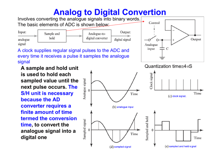
Analog to Digital Convertion Involves converting the analogue signals into binary words. The basic elements of ADC is shown below: A clock supplies regular signal pulses to the ADC and every time it receives a pulse it samples the analogue signal A sample and hold unit is used to hold each sampled value until the next pulse occurs. The S/H unit is necessary because the AD converter requires a finite amount of time termed the conversion time, to convert the analogue signal into a digital one Quantization time≅4µS AD Convertion Consider an ADC of 3 bit word then: The possible output levels is 23= 8 output levels, there ıs a range of output for which the input does not change. The 8 possible output levels are termed quantization level. The difference in analogue voltage between two adjacent levels is termed quantization interval (=1 volt in Fig.; step like nature) The digital output is not always equal to the analogue input value and thus there will be an error termed quantization error. When the input is centered over the interval, the quantization error is zero. The maximum error being equal to ½ of interval or ±½ bit Analog to Digital Convertion • The word length determine the resolution of the element: • Resolution=VFS/2n is the smallest input value which can produce 1 bit change in the output. • Eg. An ADC has 10 bits and the analogue signal input range is 10 V. The resolution is 10/1024=9.8mV Example: consider a thermocouple giving an output of 0.5 mV/C. What will be the word length required when its output passes through ADC; if temperature of 0-200 0C are to be measured with a resolution of 0.5 0C. Solution: Full scale output voltage=200x0.5=100 mV With a word length of n bit this voltage will be divided into 100/2n mV steps. For a resolution of 0.5 0C we must be able to detect a signal from the sensor of: 0.5x0.5=0.25 mV ∴ 0.25=100/2n → n=8.6 thus 9 bit word length is required Sampling theorem (1) • Nyquist’s Criteria or Shannon’s theorem – An Analog signal with a highest frequency of fa MUST be sampled at a rate fs > 2fa to avoid loss of information. – If fs < 2fa then a phenomena called aliasing will occur in the analog signal bandwidth Aliasing: When the sampling rate is less than twice the highest frequency, the reconstruction can represent some other analogue signal and we obtain a false image. An anti-aliasing filter is used precede the ADC, the filter having a band width such that it passes only low frequencies for which sampling rate will not give aliasing errors Sampling theorem (2) Aliasing examples: Analog to Digital Converter • Types: – Successive approximate – Ramp ADC /Dual Ramp – Flash Analog to Digital Converter Successive approximations ADC Successive approximations ADC is the most commonly used method. A voltage is generated by a clock emitting a regular sequence of pulses which are counted in binary manner, and the resulting word converted into an analogue voltage by DAC. This voltage rises in step and is compared with the analogue input voltage from the sensor. When the generated voltage passes the input sensor voltage, the pulses from the clock are stopped. The output from the counter at that time is the digital representation of the analogue voltage. Faster successive method is also possible Analog to Digital Converter Zero voltage terminal Successive approximations ZN439 ADC outlines Analog to Digital Converter Successive approximations ADC ZN439 connected to a microprocessor Analog to Digital Converter Ramp ADC Ramp ADC: Involve an analogue voltage which is increased at a constant rate, and applied to a comparator, where it is compared with analogue sensor voltage. When the ramp voltage starts, a gate is opened which starts a binary counter counting the regular pulses from the clock. When the two voltages are equal, the clock stop counting and the counter value indicate the equivalent digital value of the sampled one AD Flash Converter Flash ADC is very fast type of ADC .For n bit converter, 2n-1 separate voltage comparators are used in parallel, with each having the analogue input voltage as one input. The reference voltage is applied to a ladder of resistors, so the voltage applied as other input to each comparator is one bit large in size than the voltage applied to the previous comparator in the ladder Thus when the analogue voltage is applied to ADC, all those comparator for which the analogue voltage is greater than the reference voltage will give a high output and those below the reference will give a low output. The resulting output are fed in parallel to a logic gate system which translate them into a digital word Digital to Analogue Conversion A digital-to-analog converter (DAC) is a circuit that produces an analog current or voltage that is proportional to an analog reference (voltage or current) and an N-bit binary word. Vout = k x Vref x (Binary Word) Types of DAC: Weighted resistor network R-2R ladder DAC DAC Binary Weighted Principles VREF b0 b1 bn − 2 bn −1 I0 = − + n − 2 ... 1 + 0 ⇒ Vout = − I 0 R f n −1 R 2 2 2 2 I0= sum of currents leaving the junction R= resistance to LSB n= number of input bits b= bit status (1=ON or 0=OFF) DAC Example Find output voltage and current for a binary weighted resistor DAC of 4 bits where R = 10 k Ohms, Rf = 5 k Ohms and Vref = 10 Volts. Applied binary word is 1001. Solution: 10V 1 0 0 1 + 1 + 2 + 3 Io = − 0 10kΩ 2 2 2 2 I 0 = - 0.001125 A V0 = - R f I 0 V0 = −(5kΩ)(−0.001125 A) = 5.625V Limitations of the Binary Weighted DAC • A problem with the weighted resistor network is that accurate resistances have to be used for each of the resistors and its difficult to obtain such resistors over the wide range needed. As a result this form of DAC is limited to 4 bit conversion • So normally a ladder R-2R circuit which required only two accurate resistor value is used to overcome such problem R–2R ladder DAC More commonly used, only two values of resistors are required. The output is generated by switching the weighted reference voltage either to the –ive input terminal of the opamp or to the earth terminal depending on the value of the digital input binary value (0 or 1) ½I ¼I 1 8 / I / I 1 16 DAC structure ZN558D DATA ACQUISITION System (DAQ) The term DAQ is used for the process of taking data from sensors and inputting that data into a computer for processing. The basic elements of the DAQ Board is shown below: Computer software is used to control the acquisition of data via DAQ board Typical DAQ Board PC-LPM-16 DAQ board


