TCAD Based Design Methodology for Substrate Current Control in
advertisement

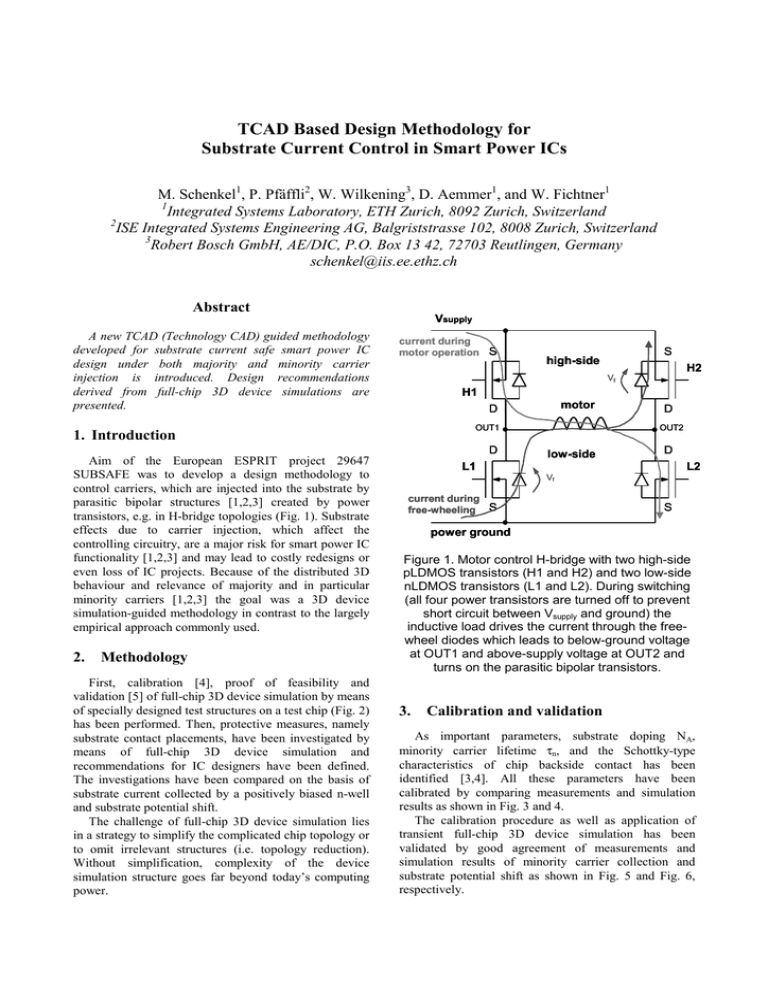
TCAD Based Design Methodology for Substrate Current Control in Smart Power ICs M. Schenkel1, P. Pfäffli2, W. Wilkening3, D. Aemmer1, and W. Fichtner1 1 Integrated Systems Laboratory, ETH Zurich, 8092 Zurich, Switzerland 2 ISE Integrated Systems Engineering AG, Balgriststrasse 102, 8008 Zurich, Switzerland 3 Robert Bosch GmbH, AE/DIC, P.O. Box 13 42, 72703 Reutlingen, Germany schenkel@iis.ee.ethz.ch Abstract A new TCAD (Technology CAD) guided methodology developed for substrate current safe smart power IC design under both majority and minority carrier injection is introduced. Design recommendations derived from full-chip 3D device simulations are presented. Vsupply current during motor operation S 2. Methodology First, calibration [4], proof of feasibility and validation [5] of full-chip 3D device simulation by means of specially designed test structures on a test chip (Fig. 2) has been performed. Then, protective measures, namely substrate contact placements, have been investigated by means of full-chip 3D device simulation and recommendations for IC designers have been defined. The investigations have been compared on the basis of substrate current collected by a positively biased n-well and substrate potential shift. The challenge of full-chip 3D device simulation lies in a strategy to simplify the complicated chip topology or to omit irrelevant structures (i.e. topology reduction). Without simplification, complexity of the device simulation structure goes far beyond today’s computing power. H2 Vf H1 motor D OUT1 1. Introduction Aim of the European ESPRIT project 29647 SUBSAFE was to develop a design methodology to control carriers, which are injected into the substrate by parasitic bipolar structures [1,2,3] created by power transistors, e.g. in H-bridge topologies (Fig. 1). Substrate effects due to carrier injection, which affect the controlling circuitry, are a major risk for smart power IC functionality [1,2,3] and may lead to costly redesigns or even loss of IC projects. Because of the distributed 3D behaviour and relevance of majority and in particular minority carriers [1,2,3] the goal was a 3D device simulation-guided methodology in contrast to the largely empirical approach commonly used. S high-side D D OUT2 low-side D L1 L2 Vf current during free-wheeling S S power ground Figure 1. Motor control H-bridge with two high-side pLDMOS transistors (H1 and H2) and two low-side nLDMOS transistors (L1 and L2). During switching (all four power transistors are turned off to prevent short circuit between Vsupply and ground) the inductive load drives the current through the freewheel diodes which leads to below-ground voltage at OUT1 and above-supply voltage at OUT2 and turns on the parasitic bipolar transistors. 3. Calibration and validation As important parameters, substrate doping NA, minority carrier lifetime τn, and the Schottky-type characteristics of chip backside contact has been identified [3,4]. All these parameters have been calibrated by comparing measurements and simulation results as shown in Fig. 3 and 4. The calibration procedure as well as application of transient full-chip 3D device simulation has been validated by good agreement of measurements and simulation results of minority carrier collection and substrate potential shift as shown in Fig. 5 and Fig. 6, respectively. n-well nLDMOS power transistor 600µ µm (L2) pLDMOS power transistor (H1) pLDMOS power transistor (H2) subcont1 950µ µm s26 test structures Figure 2. Test chip layout with four individually controllable LDMOS and a set of test structures, located where devices susceptible to substrate currents are implemented on product chips. Base-Emitter Figure 4. Minority carrier (electron) lifetime τn and substrate doping NA calibration by comparing measurements and simulation results of a parasitic NPN transistor. The collector current strongly depends on the minority carrier lifetime, which allows calibration by fitting to measurements. In the high current regime the current is limited by the substrate doping which can be calibrated, therewith. For minority carrier collection validation, minority carriers have been injected at the low-side transistor L2 and collected at the positively biased n-well located 600 µm away (Fig. 2). The substrate potential shift has been measured at the substrate contact s26 (Fig. 2) while injecting majority carriers at the 950 µm away high-side transistor H2, whereas the substrate has been grounded at the backside and the substrate contact subcont1. The achieved agreement by a factor of about 2 is considered accurate enough to make important design decisions. The accuracy is limited by the amount of finite element mesh points in the simulations. 1.E+00 1.E-01 substrate current measurement simulation 1.E-02 currents [A] 1.E-03 1.E-04 1.E-05 3 2 n-well current 1.E-06 1 drain voltage 0 1.E-07 1.E-08 Figure 3. Calibration of Schottky-type characteristic of chip backside contact. Due to formation of an unknown alloy at the chip backside the Schottky barrier height ΦBp had to be calibrated whereas the recombination velocity at the interface had to be modified to account for higher leakage current. 4 voltage [V] nLDMOS power transistor (L1) -1 1.E-09 1.E-10 -2.0E-05 -1.0E-05 0.0E+00 time [s] 1.0E-05 -2 2.0E-05 Figure 5. Validation of transient full-chip 3D device simulation by comparing measurement and simulation of transient injected minority carrier (electron) collection. measurement simulation source voltage 0.30 s26 voltage 0.20 0.15 10 0.10 0.05 5 0.00 0 subcont1 current -0.10 -0.15 -0.20 -3.E-05 -10 8.E-05 1.E-04 time [s] 2.E-04 2.E-04 Substrate contact placement 4.1. Simulation structure Figure 7 shows the application-near simulation structure used for substrate contact placement investigation. The two low-side transistors have been modelled by their minority carrier injecting buried layer to substrate junction. The majority carrier injecting parasitic PNP transistors of the high-side transistors have been replaced by p+-diffusions in the substrate. Through these p+-diffusions the substrate current determined by parasitic PNP transistor measurements has been injected. The substrate can be grounded at the Schottky-type backside contact and the substrate contacts on top. Substrate contact subcont1 is located directly in front of the high-side transistors, subcont2 behind the low-side transistors, and subcont3 adjacent to the minority carrier collecting n-well. In addition, a small, floating, substrate potential sensing substrate contact subcont4 has been placed beside the n-well. 4.2. Results Influence of different substrate grounding configurations has been investigated by comparing the current collected by a 2.6·104 µm2 n-well (Fig. 8) and the substrate potential at subcont4 (Fig. 9). Application-near below-ground and over-supply voltages and voltage slopes have been applied. Default configuration has been a grounded backside and a grounded subcont1 near the high-side power transistors. Figure 7 shows the hole quasi-fermi potential at the chip surface of the default configuration when electrons and holes are injected. The 3D nature of the problem becomes evident as the injection takes place crosswise, i.e. at L1 and H2 or at L2 and H1. subcont2 low-side 2 high-side 2 h+ subcont1 backside contact backside current Figure 6. Validation of transient full-chip 3D device simulation by comparing measurement and simulation of transient positive potential shift due to majority carrier (hole) injection. 4. high-side 1 -5 3.E-05 low-side 1 e- substrate potential sensing subcont4 15 0.25 -0.05 collecting n-well with adjacent subcont3 20 source voltage [V] currents [A], s26 voltage [V] 0.40 0.35 t = 20 µs Figure 7. Simulation structure and hole quasi-fermi potential at chip surface calculated by means of fullchip 3D device simulation. The observed quasistatic potential shift at the n-well location is negative and does not lead to junction isolation failures in the controlling circuitry. Current collection at different substrate grounding configurations in quasi-static conditions (at 20µs, Fig. 8) as well as at highly dynamic turn-off (displacement current) is listed in Table 1. Table 1. Collected n-well currents substrate quasi-static displacement n-well current n-well current [A] at turn-off [A] at 20 µs -7 subcont1, backside 1.2·10 5.0·10-5 (default) subcont2, backside 3.7·10-8 6.1·10-5 subcont1, 1.0·10-8 7.8·10-6 ohmic backside subcont1, subcont3, 2.9·10-7 1.9·10-5 backside subcont1, 3.9·10-7 5.8·10-5 without backside grounded contacts With a grounded subcont2 behind the low-side power transistors the quasi-static n-well current is almost one order of magnitude smaller than in the default configuration because of the build-up of a retarding field for electrons in the substrate, whereas the displacement current increases slightly. An ohmic backside contact leads to an even lower collected current in both cases. A grounded subcont3 near the collecting n-well results in a higher quasi-static current but in a lower displacement current because subcont3 ties the substrate to ground potential in the vicinity of the collecting n-well. Without grounded backside the quasi-static current is highest and the displacement current is also high. Collected current during quasi-static substrate current injection does not exceed 1 µA. However, capacitive displacement current during switching can reach 50 µA. effects highly depends on the specific configuration and conditions (e.g. below-ground and above-supply voltages and voltage slopes). 5. Conclusions A new methodology for substrate current safe smart power IC design has been developed, including calibration procedure with appertaining test structures, topology reduction methodology and transient full-chip 3D mixed-mode simulations. For the first time full-chip 3D device simulations of substrate current effects have been successfully validated and applied to a state-of-theart smart power technology. Design recommendations for substrate contact placement have been presented. Figure 8. Comparison of collected n-well current for different substrate grounding configurations. Substrate potential shift at quasi-static conditions is slightly negative and does not exceed –200 mV. During switching potential shifts can reach ±0.5 V and can lead to junction isolation failure, therefore. If the backside is not connected, the substrate potential shift at substrate current turn-off can even reach several volts due to the high reverse recovery current peak of the low-side buried layer to substrate junction (Fig. 9). Figure 9. Comparison of substrate potential shift for different substrate grounding configurations. Lowest collected current and substrate potential shift can be reached by an ohmic backside contact. A not connected backside leads to the highest n-well current and the highest substrate potential shift and should therefore be avoided whenever possible. Substrate contact grounding on top of the chip shows counteracting effects, e.g. a substrate contact near an n-well reduces displacement current and substrate potential shift but increases the quasi-static current. The magnitude of these 6. Acknowledgement This work has been funded by the European Commission under ESPRIT Project 29647 SUBSAFE (Substrate Current Safe Smart-Power IC Design Methodology) [6] and the Swiss Office for Education and Science. 7. References [1] B. Murari, F. Bertotti, G.A. Vignola, Smart Power ICs: Technologies and Applications, Springer, Berlin, 1996 [2] C. Contiero, P. Galbiati, M. Palmieri, G. Ricotti, R. Stella, “Smart Power Approaches VLSI Complexity”, Proceedings of 1998 International Symposium on Power Semiconductor Devices & ICs, Kyoto, 1998, pp. 11-16 [3] R.J. Widlar, “Controlling Substrate Currents in Junction-Isolated IC's”, IEEE Journal of Solid-State Circuits, Vol. 26, No. 8, August 91, pp. 1090-1097 [4] M. Schenkel, P. Pfäffli, W. Wilkening, D. Aemmer, W. Fichtner, “Substrate Potential Shift due to Parasitic Minority Carrier Injection in Smart-Power ICs: Measurements and Full-Chip 3D Device Simulation”, Microelectronics Reliability, Pergamon, Vol. 41, No. 6, June 2001, pp. 815-822 [5] M. Schenkel, P. Pfäffli, W. Wilkening, D. Aemmer, W. Fichtner, “Transient Minority Carrier Collection from the Substrate in Smart Power Design”, Proceedings of ESSDERC ‘01, Nuremberg, 2001, pp. 411-414 [6] SUBSAFE (Substrate Current Safe Smart Power IC Design Methodology), ESPRIT Project 29647, http://www.iis.ee.ethz.ch/nwp/subsafe/index.html

