Chip on board – Wire Bonding Design Rules
advertisement
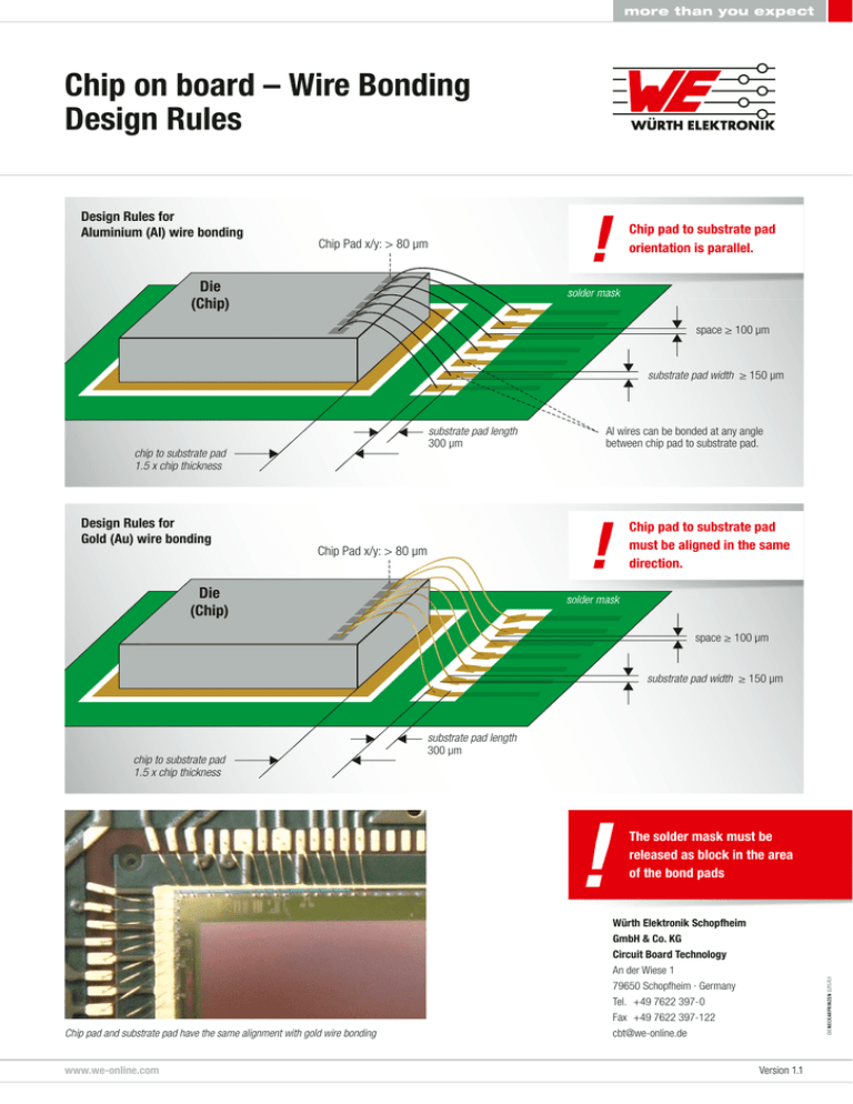
Chip on board – Wire Bonding Design Rules Design Rules for Aluminium (Al) wire bonding Chip pad to substrate pad orientation is parallel. Chip Pad x/y: > 80 µm Die (Chip) solder mask space ≥ 100 μm substrate pad width ≥ 150 μm substrate pad length 300 μm chip to substrate pad 1.5 x chip thickness Design Rules for Gold (Au) wire bonding Al wires can be bonded at any angle between chip pad to substrate pad. Chip pad to substrate pad must be aligned in the same direction. Chip Pad x/y: > 80 µm Die (Chip) solder mask space ≥ 100 μm substrate pad width ≥ 150 μm chip to substrate pad 1.5 x chip thickness substrate pad length 300 μm The solder mask must be released as block in the area of the bond pads www.we-online.com DIENECK ARPRINZEN 0215.FLY Chip pad and substrate pad have the same alignment with gold wire bonding Würth Elektronik Schopfheim GmbH & Co. KG Circuit Board Technology An der Wiese 1 79650 Schopfheim · Germany Tel. +49 7622 397-0 Fax +49 7622 397-122 cbt@we-online.de Version 1.1
