4-bit Carry Ripple Adder
advertisement

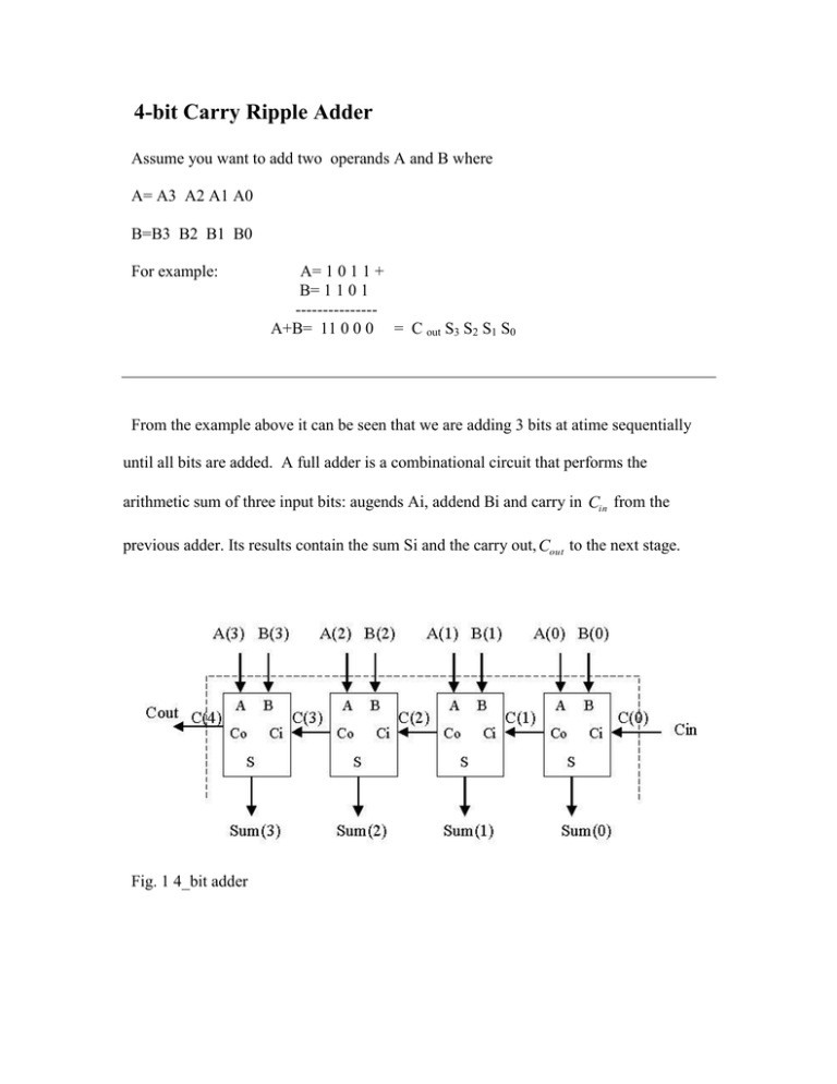
4-bit Carry Ripple Adder Assume you want to add two operands A and B where A= A3 A2 A1 A0 B=B3 B2 B1 B0 For example: A= 1 0 1 1 + B= 1 1 0 1 --------------A+B= 11 0 0 0 = C out S3 S2 S1 S0 From the example above it can be seen that we are adding 3 bits at atime sequentially until all bits are added. A full adder is a combinational circuit that performs the arithmetic sum of three input bits: augends Ai, addend Bi and carry in Cin from the previous adder. Its results contain the sum Si and the carry out, Cout to the next stage. Fig. 1 4_bit adder So to design a 4-bit adder circuit we start by designing the 1 –bit full adder then connecting the four 1-bit full adders to get the 4-bit adder as shown in the diagram above. For the 1-bit full adder, the design begins by drawing the Truth Table for the three input and the corresponding output SUM and CARRY. The Boolean Expression describing the binary adder circuit is then deduced. The binary full adder is a three input combinational circuit which satisfies the truth table below. Fig.2. Diagram and Truth Table of Full Adder The Boolean equations of a full adder are given by: Sout = ABC + AB’C’ + A’B’C + BA’C’ =(AB’+BA’)C +AB+A’B’) C’ Sout = A⊕B⊕C Cout = AB + AC + BC Cout = AB + C (A⊕B) The circuit diagram is shown in Fig.3 and the simulation results is shown in Fig. 4 Fig. 3. The Gate level Diagram of Full Adder Fig. 4 1 bit full adder simulation results To design a 4-bit adder now we cascade 4 1-bit adders as shown in Fig. 5 A2 A2 A2 A2 FA B2 FA FA FA B2 B2 B2 C2 C2 C2 C2 S2 S2 S2 S2 Fig. 5 4-bit Ripple Carry adder As is seen from Fig. 5 and Fig. 6 the carry ripples through the 4 full adders to appear at the output, while the sums are available after 2 XOR delay. B3 Cout A3 FA B2 C2 S3 A2 FA B1 C1 S2 A1 FA S1 B0 C0 A0 FA Cin S0 Fig. 5 Carry Propagation The carry propagation is shown in Fig. 5 as a block and as a path through the circuit in Fig. 6 Fig. 6 carry propagation through the circuit

