AN39 - Parasitic Capacitance Effects in Step
advertisement
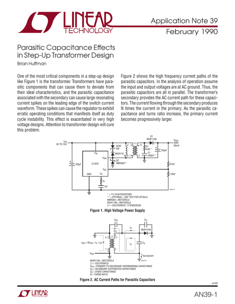
Application Note 39 February 1990 Parasitic Capacitance Effects in Step-Up Transformer Design Brian Huffman One of the most critical components in a step-up design like Figure 1 is the transformer. Transformers have parasitic components that can cause them to deviate from their ideal characteristics, and the parasitic capacitance associated with the secondary can cause large resonating current spikes on the leading edge of the switch current waveform. These spikes can cause the regulator to exhibit erratic operating conditions that manifests itself as duty cycle instability. This effect is exacerbated in very high voltage designs. Attention to transformer design will cure this problem. Figure 2 shows the high frequency current paths of the parasitic capacitors. In the analysis of operation assume the input and output voltages are at AC ground. Thus, the parasitic capacitors are all in parallel. The transformer’s secondary provides the AC current path for these capacitors. The current flowing through the secondary produces N times the current in the primary. As the parasitic capacitance and turns ratio increase, the primary current becomes progressively larger. D1 MUR1100 VIN 8V TO 15V 4 5 5A30 3W VIN MUR110 VSW + 8 7• • 11 R1 + 6.8k** C1 200pF** 2 D2 MBR360** LT1070 100μF • L1 VOUT 330V 50mA 100μF 475k* VFB GND VC 1.82k* 1k 1μF AN39 F01 * = 1% FILM RESISTORS ** = OPTIONAL—SEE TEXT FOR DETAILS MBR360 = MOTOROLA MUR1100 = MOTOROLA L1 = COILTRONICS* CTX30203C04 Figure 1. High Voltage Power Supply CPS CD ID IPS MUR1100 • 4, 5 L1 11 IPRI = N(IPS + IS + ID) IS 7, 8 VSW • CS 2 ISECONDARY AN39 F02 MUR1100 = MOTOROLA L1 = COILTRONICS CPS = PRIMARY-TO-SECONDARY INTERWINDING CAPACITANCE CS = SECONDARY DISTRIBUTED CAPACITANCE CD = DIODE CAPACITANCE N = TURNS RATIO Figure 2. AC Current Paths for Parasitic Capacitors an39f AN39-1 Application Note 39 The operation waveforms for this circuit are shown in Figure 3. When the switch (VSW pin—Trace A) is turned “on” the primary is pulled to ground. The secondary cannot instantly follow this action because of the loading effects of its parasitic capacitors. The effects of the parasitic capacitance can easily be seen in the leading edge of the switch current waveform (Trace B). This current spike is caused by the loading effect of the secondary parasitic capacitances. The secondary output (Trace D) swing can exceed 600V. As such, a large amount of charge (Q = C • V) is needed to swing this node during the switching transients. The secondary current is amplified by the turns ratio and produces a primary current; IPRI = N(IPS + IS + ID). This amplifying effect can be observed by comparing the secondary current (Trace C), which does not include the effects of IS, with the switch current (Trace B). The result is a rather large current spike. The oscillatory nature of the response is formed by a series combination of the leakage inductance and reflected secondary capacitance (Figure 4). Any impedance placed across the secondary appears at the primary terminals reduced in magnitude by a factor of the turns ratio squared. For example, if N = 10, then a 200Ω resistor looks like 2Ω and a 100pF capacitor looks like 0.01μF, so even a small secondary capacitance can heavily load the primary. The series LC forms a self-resonating circuit that rings at the resonant frequency of the transformer. The output switching diode, D1, can also cause narrow spikes on the current waveform. In this case, the reverse recovery time of the diode is the important parameter. Reverse recovery time occurs because the diode “stores” charge during its forward conducting cycle. This stored charge causes the diode to act like a low impedance conductive element for a short period of time after reverse drive is applied. There is a short period of time (blanking time) following switch turn “on” during which the LT1070 ignores the switch current waveform. This blanking time eliminates premature termination of the “on” pulse caused by the leading edge current spike in the current waveform. Once this blanking time has elapsed the output switch will turn “off” when the peak switch current reaches the threshold level established by the error amplifier output (VC pin). VIN VSW A = 50V/DIV LLEAKAGE VIN VSW B = 2A/DIV ISW C = 0.5A/DIV ISECONDARY N2 • (CS + CPS + CD) LT1070 GND AN39 F04 D = 200V/DIV VSECONDARY HORIZ = 5μs/DIV Figure 4. Simplified Primary Model During Transient Conditions AN39 F03 Figure 3. Operating Waveforms for High Voltage Converter an39f AN39-2 Application Note 39 This internally fixed blanking time, 400ns, is appropriate for typical applications. However, for high voltage applications the blanking time becomes a critical parameter. The effects of the transformer’s parasitic capacitance is to extend the “spike” width past the blanking time causing the LT1070 to mistrigger, as shown in Figure 5. The duty cycle variations in the switch pin (Trace A) and switch current (Trace B) waveforms are the result of this problem. Figure 6 details the interaction between blanking time and peak switch current. Notice that the switch is turned “off” as soon as the LT1070 samples the switch current. For the LT1070 to function properly, the spike current must be below the normal peak switch current before the 400ns blanking period is over. Another problem induced by the parasitic capacitance can also be seen in Figure 3. High reverse current can flow in the VSW pin (Trace B) due to the oscillatory nature of the transformer. This will forward bias the LT1070’s substrate diode, which is inherent in the output transistor (see Appendix A). Unwanted current can flow almost anywhere within the IC’s circuitry when the substrate diode is forward biased, causing unpredictable duty cycle behavior. A = 20V/DIV VSW B = 1A/DIV ISW The substrate diode current can be eliminated by placing a Schottky diode, D2, between the VSW pin and ground (Figure 1). The reverse primary current will flow through the Schottky diode instead of the LT1070. Another way to prevent the substrate diode from conducting is to place an RC snubber, R1-C1, on the secondary. This will attenuate the ringing. Well known transformer winding techniques can be used to minimize parasitic capacitance in step-up transformers. The basic technique is to wind the secondary layers in a manner that minimizes the voltage difference between adjacent layers. A standard way of accomplishing this is to wind several separate secondary “stacks” on a split bobbin. This and other techniques will cause a dramatic reduction in secondary capacitance. For transformer information contact: Coiltronics 984 Southwest 13th Court Pompano Beach, FL 33069 305-781-8900 A = 20V/DIV VSW B = 2A/DIV ISW HORIZ = 20μs/DIV HORIZ = 2μs/DIV Figure 5. Duty Cycle Instability Due to Current Spike Figure 6. Detail Waveforms of Switch Current Spike an39f Information furnished by Linear Technology Corporation is believed to be accurate and reliable. However, no responsibility is assumed for its use. Linear Technology Corporation makes no representation that the interconnection of its circuits as described herein will not infringe on existing patent rights. AN39-3 Application Note 39 APPENDIX A If the vertical NPN output switch transistor is operating in its normal mode, either “on” or “off,” the parasitic transistor is off and will have no effect. The parasitic becomes active when the vertical collector is pulled to a potential below that of the substrate by the reverse switch current. This forward biases the collector substrate junction, which is commonly called the substrate diode. As a result, the parasitic NPN draws current from other portions of the circuit. This current will add to the base drive of lateral PNPs and to the collector current of NPNs, causing the IC to behave in mysterious and unpredictable ways (see Figure A2). In a junction isolated IC the monolithic transistors are surrounded by an isolating P-N junction, as illustrated in Figure A1. When this junction is reverse biased, it electrically isolates one device from another on the chip. However, this device structure also forms parasitic lateral NPN transistors (see Figure A2). The P substrate is the base, the N-epi region is the emitter and the collector is any other N-epi pocket. A simplified schematic diagram of the NPN cell is shown in Figure A3. EMITTER BASE N+ COLLECTOR N+ P P P N– N+ AN39 FA1 P SUBSTRATE TIED TO GROUND PIN OF LT1070 Figure A1. Junction Isolated NPN Structure (LATERAL PNP) COLLECTOR P P EMITTER Q1 P (VERTICAL NPN) COLLECTOR Q1 P BASE ISOLATION WALL N+ EMITTER BASE N+ P (VERTICAL NPN) ISOLATION WALL COLLECTOR N+ P N– EMITTER BASE N+ P N+ P N– N+ P N– N+ N+ PARASITIC NPN COLLECTOR AN39 FA2 PARASITIC NPN P SUBSTRATE Figure A2. Locations Where the Lateral NPN Occur VSW (LT1070 SWITCH PIN) ANY POCKET IN THE CIRCUIT LT1070 OUTPUT SWITCH PARASITIC LATERAL NPN BASE SUBSTRATE LT1070 GROUND PIN AN39 FA3 Figure A3. Schematic Diagram of LT1070’s Output Switch with Parasitic an39f AN39-4 Linear Technology Corporation IM/GP 290 20K • PRINTED IN USA 1630 McCarthy Blvd., Milpitas, CA 95035-7417 (408) 432-1900 ● FAX: (408) 434-0507 ● www.linear.com © LINEAR TECHNOLOGY CORPORATION 1990
