AN-835 Differential Input with VCMR being VIH Referenced
advertisement

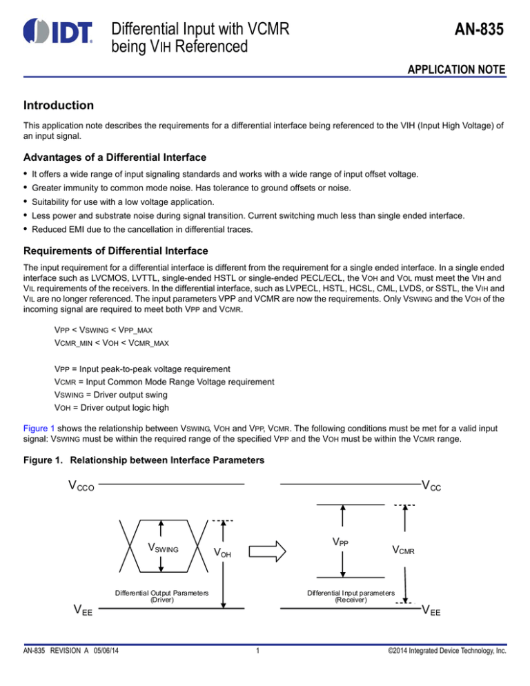
Differential Input with VCMR being VIH Referenced AN-835 APPLICATION NOTE Introduction This application note describes the requirements for a differential interface being referenced to the VIH (Input High Voltage) of an input signal. Advantages of a Differential Interface • • • • • It offers a wide range of input signaling standards and works with a wide range of input offset voltage. Greater immunity to common mode noise. Has tolerance to ground offsets or noise. Suitability for use with a low voltage application. Less power and substrate noise during signal transition. Current switching much less than single ended interface. Reduced EMI due to the cancellation in differential traces. Requirements of Differential Interface The input requirement for a differential interface is different from the requirement for a single ended interface. In a single ended interface such as LVCMOS, LVTTL, single-ended HSTL or single-ended PECL/ECL, the VOH and VOL must meet the VIH and VIL requirements of the receivers. In the differential interface, such as LVPECL, HSTL, HCSL, CML, LVDS, or SSTL, the VIH and VIL are no longer referenced. The input parameters VPP and VCMR are now the requirements. Only VSWING and the VOH of the incoming signal are required to meet both VPP and VCMR. VPP < VSWING < VPP_MAX VCMR_MIN < VOH < VCMR_MAX VPP = Input peak-to-peak voltage requirement VCMR = Input Common Mode Range Voltage requirement VSWING = Driver output swing VOH = Driver output logic high Figure 1 shows the relationship between VSWING, VOH and VPP, VCMR. The following conditions must be met for a valid input signal: VSWING must be within the required range of the specified VPP and the VOH must be within the VCMR range. Figure 1. Relationship between Interface Parameters V CCO V CC VSWING VPP VOH Differential Output Parameters (Driver) Differential Input parameters (Receiver) V EE AN-835 REVISION A 05/06/14 VCMR V EE 1 ©2014 Integrated Device Technology, Inc. AN-835 Figure 2. Typical Datasheet for VCMR and VPP Example Figure 2 shows a typical datasheet specification for both VPP and VCMR. As an example, let’s use an input driver with an amplitude (VSWING) of 200mV and a VOH level at 2V. Will this work? First, the VSWING should be verified that it is within the VPP specification. Yes, 200mV falls between 0.15V and 1.3V. Second, the VOH of the signal must fall within the VCMR range. Assuming the VCC is 3.3V and VEE is 0V, the VCMR range will be 0.5V and 2.45V. Again, 2V fall within the VCMR range. Both of the conditions are met. This is a valid input. Though not specified, it is not recommended that the VIL goes below VEE. This could happen with the VPP at 1.3V and the VIH at VEE+0.5. That would put the VIL at 800mV below VEE. Limitations of VCMR and VPP This section will describe the limitation of both VCMR and v from a circuit perspective. When VCMR is referenced to VIH, the analysis is purely DC. Some inputs also reference VCMR to the input signals cross-point. This would be a similar except it would be an AC analysis. Figure 3. Simplified Typical Differential Input Interface Circuit VC C A R1 R2 VOU T - V IN + V C MR B Q1 VOU T + Q2 C V PP E V IN I1 C urren t S ource D V EE For the following analysis, refer to Figure 3. In determining VPP, both VPP(min) and VPP(max) specification must be examined. For both cases, VIN+ is greater than VIN-, where VIN+ is a logic high and VIN- is a logic low. • VPP(min) is determined by the minimum voltage difference required to correctly operate the differential amplifier by keeping the Q1 transistor on and Q2 off. • VPP(max) is determined by the maximum voltage swing allowable which will not forward bias either Q1 or Q2. Similar to VPP, both VCMR(max) and VCMR(min) must be examined. • VCMR(min) is determined by the minimum VCD required to keep the constant current source I1 function properly. • VCMR(max) is determined by the minimum VAB required to prevent the forward biasing of Q1. DIFFERENTIAL INPUT WITH VCMR BEING VIH REFERENCED 2 REVISION A 05/06/14 Corporate Headquarters Sales Tech Support 6024 Silver Creek Valley Road San Jose, CA 95138 USA 1-800-345-7015 or 408-284-8200 Fax: 408-284-2775 www.IDT.com email: clocks@idt.com DISCLAIMER Integrated Device Technology, Inc. (IDT) and its subsidiaries reserve the right to modify the products and/or specifications described herein at any time and at IDT’s sole discretion. All information in this document, including descriptions of product features and performance, is subject to change without notice. Performance specifications and the operating parameters of the described products are determined in the independent state and are not guaranteed to perform the same way when installed in customer products. The information contained herein is provided without representation or warranty of any kind, whether express or implied, including, but not limited to, the suitability of IDT’s products for any particular purpose, an implied warranty of merchantability, or non-infringement of the intellectual property rights of others. This document is presented only as a guide and does not convey any license under intellectual property rights of IDT or any third parties. IDT’s products are not intended for use in applications involving extreme environmental conditions or in life support systems or similar devices where the failure or malfunction of an IDT product can be reasonably expected to significantly affect the health or safety of users. Anyone using an IDT product in such a manner does so at their own risk, absent an express, written agreement by IDT. Integrated Device Technology, IDT and the IDT logo are registered trademarks of IDT. Product specification subject to change without notice. Other trademarks and service marks used herein, including protected names, logos and designs, are the property of IDT or their respective third party owners. Copyright ©2014 Integrated Device Technology, Inc.. All rights reserved.


