Tunnel Diode - in a heavily doped p-n junction the depletion region
advertisement

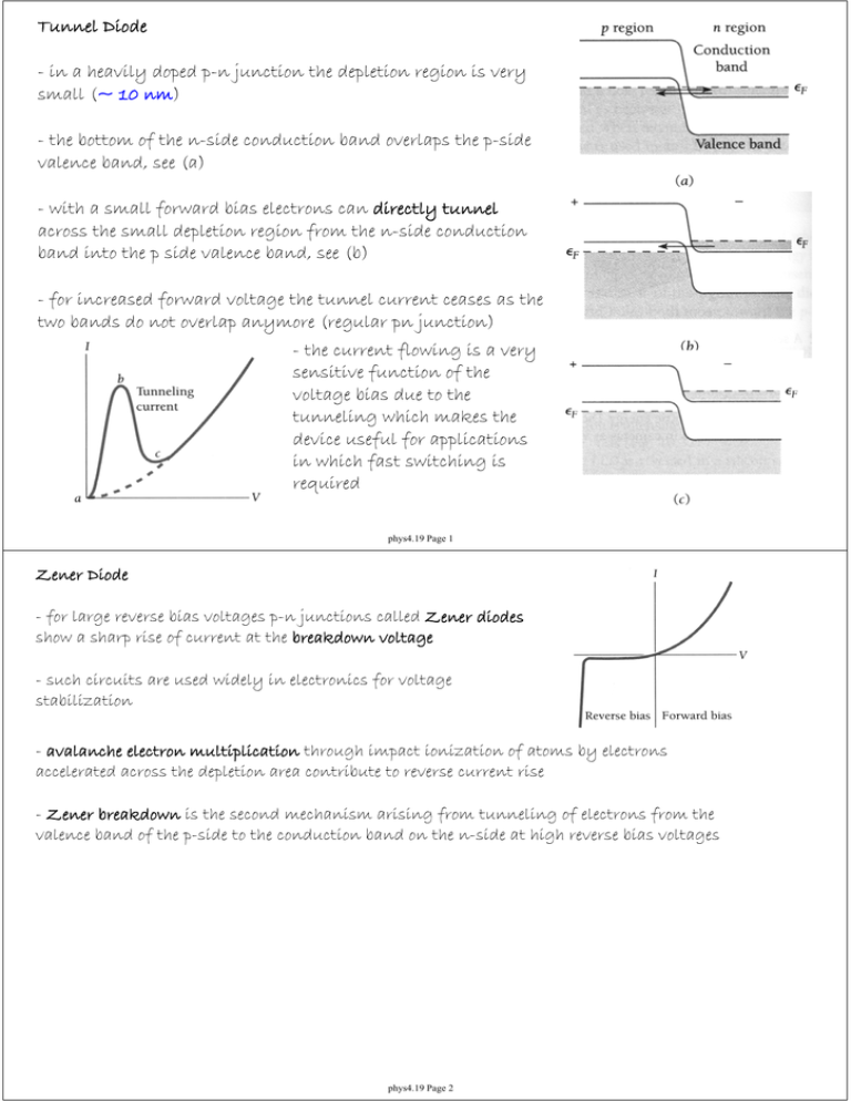
Tunnel Diode - in a heavily doped p-n junction the depletion region is very small (~ 10 nm) - the bottom of the n-side conduction band overlaps the p-side valence band, see (a) - with a small forward bias electrons can directly tunnel across the small depletion region from the n-side conduction band into the p side valence band, see (b) - for increased forward voltage the tunnel current ceases as the two bands do not overlap anymore (regular pn junction) - the current flowing is a very sensitive function of the voltage bias due to the tunneling which makes the device useful for applications in which fast switching is required phys4.19 Page 1 Zener Diode - for large reverse bias voltages p-n junctions called Zener diodes show a sharp rise of current at the breakdown voltage - such circuits are used widely in electronics for voltage stabilization - avalanche electron multiplication through impact ionization of atoms by electrons accelerated across the depletion area contribute to reverse current rise - Zener breakdown is the second mechanism arising from tunneling of electrons from the valence band of the p-side to the conduction band on the n-side at high reverse bias voltages phys4.19 Page 2 npn-Junction Transistor - consists of a thin p-doped region called the base electrode connected to an n-doped emitter and collector electrode, see figure - an npn transistor acts as an amplifier for small signals applied between the emitter and base electrode that are amplified into a large base-collector signals - the energy band structure of the npn transistor at zero bias is shown - the current in an npn transistor is carried by electrons - a pnp transistor would work in an analog way for holes being the predominant charge carrier phys4.19 Page 3 Transistor Bias - for transistor operation the emitter base junction is weakly forward biased and the base collector junction is strongly reverse biased - the current from the heavily doped emitter into the base is carried by electrons - electrons diffuse across the thin (~ 1 μm) weakly hole doped base electrode into the baseemitter junction and are accelerated by the large reverse bias into the collector - the input signal power is then amplified at constant current by the large base collector reverse bias voltage to a larger output power - a limitation of the npn transistor amplifier is its low input impedance (or low input resistance), also its power consumption and integration density are not the best - for some applications an amplifier with higher input impedance, such as a field effect transistor, is advantageous phys4.19 Page 4 Field Effect Transistor (FET) - an FET consists of a n-type channel connecting source and drain and contacted by a p-type gate; it is widely used as an alternative to npn junction transistors - electrons move from source to drain along an n-type channel - the pn junction is reverse biased to create a depletion region at the interface, the carrier density and the source-drain current depend sensitively on the magnitude of the reverse bias - in reverse bias little current flows into the pn junction giving it a high input impedance Metal Oxide Semiconductor Field Effect Transistor (MOSFET) - semiconductor gate replaced by a metal film separated from the channel by a thin oxide layer - MOSFETs have high input impedance (up to 1015 Ω) due to capacitively coupled gate and are also compatible with high integration density phys4.19 Page 5 Superconductivity - usual electrical conductors, even the very best ones, have finite resistance determined by temperature and impurities in the material - at very low temperatures some metals, alloys and some special chemical compounds can transport current without resistance, an effect called superconductivity - Kammerlingh Onnes discovered that resistance of mercury (Hg) decreased like that of other metals down to Tc ~ 4.15 K but then lost all of its resistance to immeasurable levels below that critical temperature Tc - the resistivity is actually zero as tested in persistent current measurements - usual critical temperatures for metallic superconductors are in the range 0.1 - 10 K - it is interesting to note that good usual conductors such as copper (Cu) and silver (Ag) do not become superconducting phys4.19 Page 6 The Nobel Prize in Physics 1913 "for his investigations on the properties of matter at low temperatures which led, inter alia, to the production of liquid helium" Leiden University, Leiden, the Netherlands Heike Kamerlingh Onnes b. 1853, d. 1926 The Nobel Prize in Physics 1987 "for their important break-through in the discovery of superconductivity in ceramic materials" IBM Zurich Research Laboratory Rüschlikon, Switzerland J. Georg Bednorz Germany b. 1950 K. Alexander Müller Switzerland b. 1927 phys4.19 Page 7 Magnetic Effects - the critical temperature Tc of a superconductor depends on the magnetic field (see figure) - in a type I superconductor the zero resistance state disappears altogether at a threshold critical field Bc that depends on the material and the temperature - the maximum critical field occurs at zero temperature Superconductor Tc and Bc - because of the limited critical fields of type I superconductors they are of limited use in applications for field generation with coils phys4.19 Page 8 material Al Hg In Pb Sn Zn Tc [K] 1.18 4.15 3.41 7.19 3.72 0.85 Bc [T] 0.015 0.041 0.028 0.080 0.031 0.005 Meissner Effect - superconductors are perfectly diamagnetic - in a type I superconductor field below the critical field is expelled completely from the material when cooled through Tc , see figure - in this Meissner effect screening currents are induced in the superconductor to cancel the externally applied field - this effect distinguishes a superconductor from an ideal conductor - type II superconductors below a first critical field Bc1 behave like type I superconductors, above Bc1 and below a second critical field Bc2 magnetic flux can penetrate into the material bringing it to a mixed superconducting/normal state - Bc2 critical fields can be high so that these materials are interesting for generating magnetic fields material Nb3Sn Tc [K] 18.0 Bc2 [T] 24.5 phys4.19 Page 9 Cooper Pairs and Bardeen-Cooper-Schrieffer (BCS) theory - in conventional superconductors electrons attract each other through deformations induced in the crystal lattice - materials with strong lattice vibrations are usually poor conductors at room temperature but maybe superconductors at low temperatures - a hint of this fact was first found when it was noted that the Tc of different superconductors depends on the isotope used, e.g. Tc(199Hg) = 4.161 and Tc(204Hg) = 4.126 - two electrons (Fermions) form a single Cooper pair (Boson) with the electrons being in a singlet state with zero angular momentum - the binding energy Eg, also called the gap energy, is typically on the order of 1 meV and can be measured using microwave absorption - at temperatures above 0 K some Cooper pairs are broken up by thermal fluctuations, the remaining electrons interact with the Cooper pairs effectively reducing the gap energy (see figure) phys4.19 Page 10 - at the critical temperature Tc the energy gap disappears, there are no more Cooper pairs and thus the material ceases to be superconducting - electrons (fermions) in a superconductor form Cooper pairs with total spin S = 0 - the Cooper pair is a boson, any number of bosons can be in the same quantum state ψ - Cooper pairs in a super conductor form a Bose-Einstein condensate - all Cooper pairs in a superconductor are described by a single macroscopic wave function minimizing the system energy where ρ is the Cooper pair density and φ their phase - when a current flows in a superconductor, all Cooper pairs have the same non-zero linear momentum - no scattering of individual electrons that would lead to finite resistance can occur phys4.19 Page 11 Flux Quantization - Faraday's law relates the current I flowing through a loop enclosing an area A and the magnetic flux Φ = A B in the loop - the flux Φ in the superconductor is quantized because the wave function describing the Cooper pairs in the ring must be a continuous periodic function around the loop (compare to Bohr model) - the flux quantization rule is - with the magnetic flux quantum phys4.19 Page 12


