Energy Band Bending Profile of Ultra-Shallow Junction in - SPring-8
advertisement

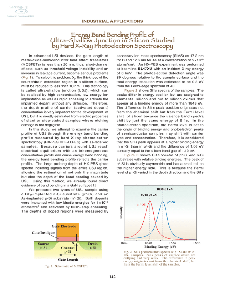
Industrial Applications Energy Band Bending Profile of Ultra-Shallow Junction in Silicon Studied by Hard X-Ray Photoelectron Spectroscopy In advanced LSI devices, the gate length of metal-oxide-semiconductor field effect transistors (MOSFETs) is less than 20 nm; thus, short-channel effects, such as threshold-voltage instability and an increase in leakage current, become serious problems (Fig. 1). To solve this problem, Xj, the thickness of the source/drain extension region in a silicon surface, must be reduced to less than 10 nm. This technology is called ultra-shallow junction (USJ), which can be realized by high-concentration, low-energy ion implantation as well as rapid annealing to activate the implanted dopant without any diffusion. Therefore, the depth profile of carrier (activated dopant) concentration is very important for the development of USJ, but it is mostly estimated from electric properties of slant or step-etched samples where etching damage is not negligible. In this study, we attempt to examine the carrier profile of USJ through the energy band bending profile measured by hard X-ray photoelectron spectroscopy (HX-PES or HAXPES) with as-received samples. Because carriers around USJ reach electrical equilibrium with an inhomogeneous concentration profile and cause energy band bending, the energy band bending profile reflects the carrier profile. The large probing depth of HX-PES gives spectra including signals from the entire USJ region, allowing the estimation of not only the magnitude but also the depth of the band bending caused by USJ. Using this method, we already found direct evidence of band bending in a GaN surface [1]. We prepared two types of USJ sample using a BF 2 -implanted n-Si substrate (p + -Si) and an As-implanted p-Si substrate (n+-Si). Both dopants were implanted with low kinetic energies for 1 × 10¹⁵ atoms/cm 2 and activated by flush-lamp annealing. The depths of doped regions were measured by secondary ion mass spectroscopy (SIMS) as 17.2 nm for B and 12.6 nm for As at a concentration of 5 ×10¹⁸ atoms/cm3. An HX-PES experiment was performed at beamline BL47XU with an incident X-ray energy of 8 keV. The photoelectron detection angle was 89 degrees relative to the sample surface and the total energy resolution was estimated to be 0.3 eV from the Fermi-edge spectrum of Au. Figure 2 shows Si1s spectra of the samples. The peaks differ in energy position but are assigned to elemental silicon and not to silicon oxides that appear at a binding energy of more than 1843 eV. The difference in Si1s peak position originates not from the chemical shift but from the Fermi level shift of silicon because the valence band spectra shift by just the same energy of Si1 s . In the photoelectron spectrum, the Fermi level is set to the origin of binding energy and photoelectron peaks of semiconductor samples may shift with carrier type and concentration. Therefore, it is considered that the Si1s peak appears at a higher binding energy in n+-Si than in p+-Si and the difference of 1.06 eV is nearly equal to the silicon band gap of 1.12 eV. Figure 3 shows Si1s spectra of p+-Si and n-Si substrates with relative binding energies. The peak of p+-Si is obviously asymmetric and has a small tail on the higher energy side. This is because the Fermi level of p+-Si varied in the depth direction and the Si1s 1838.81 eV 1839.87 eV p+-Si Intensity n+-Si Gate Electrode Gate Insulator Source n-Si Xj Channel p-Si 1842 Drain n-Si 1840 1838 Binding Energy (eV) 1836 Fig. 2. Si1s photoelectron spectra of p+-Si and n+-Si USJ samples. Si1s peaks of surface oxide are outlying and very weak. The difference in peak energy originates not from the chemical shift, but from the Fermi level shift of the samples. Gate Length Fig. 1. Schematic of MOSFET. 142 Intensity p+-Si n-Si substrate 3 2 1 0 –1 –2 Relative Binding Energy (eV) –3 Fig. 3. Si1s photoelectron spectra of p+-Si USJ sample and n-Si substrate. The spectra are calibrated with a peak energy of 0.0 eV and normalized with peak height. In the case of a GaN surface, the N1s spectrum showed a large asymmetric peak and we could derive its energy band bending profile by peak deconvolution [1,2]. However, the band gap of silicon is smaller than that of GaN and the degree of energy band bending also decreases. Consequently, an HX-PES experiment with a higher energy resolution is necessary for obtaining precise energy band bending profiles of silicon. spectrum consisted of peaks with different energy positions originating from the probing depths of HX-PES. When a thin p+-Si layer is activated by many carriers, the difference in Fermi level between the p +-Si and n-Si substrates is about 1 eV; thus, the migration of carriers results in energy band bending (Fig. 4). This suggests that HX-PES can provide both the magnitude and depth of energy band bending in silicon with USJ. 1.5 1.0 HX-PES probing depth Potential (eV) 0.5 CBM 0.0 – 0.5 VBM magnitude of band bending 1839 Si 1s 1840 0 depth of band bending 5 10 15 20 Depth (nm) 25 30 Fig. 4. Example of energy band diagram for p+-Si USJ sample. Note that the depth scale is incorrect here. References [1] M. Yoshiki, S. Saito, S. Nunoue, E. Ikenaga, K. Kobayashi: User Exp. Report, 2005B0807 (in Japanese). [2] M. Yoshiki, M. Suzuki, Y. Tsuchiya, R. Ichihara, S. Saito, S. Takeno: Houshyakou 22(1) (2009) 20 (in Japanese). Masahiko Yoshiki Corporate Research & Development Center, Toshiba Corporation E-mail : masahiko.yoshiki@toshiba.co.jp 143
