Designer Project
advertisement
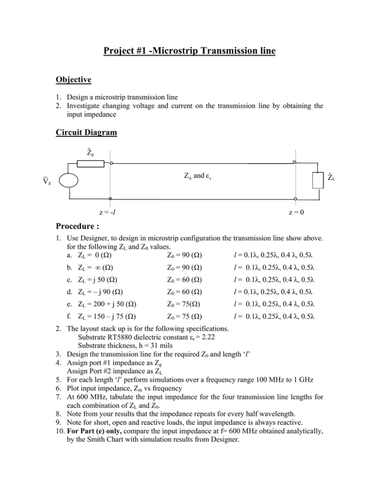
Project #1 -Microstrip Transmission line Objective 1. Design a microstrip transmission line 2. Investigate changing voltage and current on the transmission line by obtaining the input impedance Circuit Diagram Ẑg Z 0 and ε r ~ Vg z = -l ẐL z=0 Procedure : 1. Use Designer, to design in microstrip configuration the transmission line show above. for the following ZL and Z0 values. a. ZL = 0 (Ω) Z0 = 90 (Ω) l = 0.1λ, 0.25λ, 0.4 λ, 0.5λ b. ZL = ∞ (Ω) Z0 = 90 (Ω) l = 0.1λ, 0.25λ, 0.4 λ, 0.5λ c. ZL = j 50 (Ω) Z0 = 60 (Ω) l = 0.1λ, 0.25λ, 0.4 λ, 0.5λ d. ZL = – j 90 (Ω) Z0 = 60 (Ω) l = 0.1λ, 0.25λ, 0.4 λ, 0.5λ e. ZL = 200 + j 50 (Ω) Z0 = 75(Ω) l = 0.1λ, 0.25λ, 0.4 λ, 0.5λ f. ZL = 150 – j 75 (Ω) Z0 = 75 (Ω) l = 0.1λ, 0.25λ, 0.4 λ, 0.5λ 2. The layout stack up is for the following specifications. Substrate RT5880 dielectric constant εr = 2.22 Substrate thickness, h = 31 mils 3. Design the transmission line for the required Z0 and length ‘l’ 4. Assign port #1 impedance as Zg Assign Port #2 impedance as ZL 5. For each length ‘l’ perform simulations over a frequency range 100 MHz to 1 GHz 6. Plot input impedance, Zin vs frequency 7. At 600 MHz, tabulate the input impedance for the four transmission line lengths for each combination of ZL and Z0. 8. Note from your results that the impedance repeats for every half wavelength. 9. Note for short, open and reactive loads, the input impedance is always reactive. 10. For Part (e) only, compare the input impedance at f= 600 MHz obtained analytically, by the Smith Chart with simulation results from Designer. Ansoft Designer Tutorial 1.Open Ansoft Designer 2.Project/Insert Circuit Design 3.‘None’ 4. Schematic/Layout Stackup 5. “Add Layer” 6.Name: Ground Type: MetalizedSignal 7.Repeat steps 5-6, for: Name: Dielectric Type: Dielectric Name: Trace Type: Signal 8.Change the material for the Dielectric layer Click on “Rogers R…” Select “Add Material…” Enter values for Dielectric Layer Click ‘Ok’ twice 9.Check materials for the Trace and ground layers. (Copper unless otherwise specified) If it is different, repeat Step 8 for each material. 10. Change the Thickness of the Dielectric and Trace layers to the specified values. (0.675mil and 31mil are standard for the Rogers Duriod 5870) 11. Select ‘Ok’
