Low-Voltage, Vertical-Junction, Depletion
advertisement

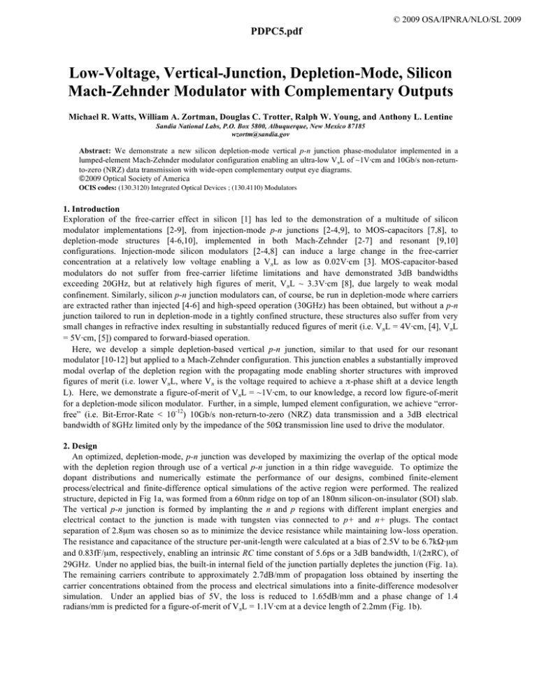
© 2009 OSA/IPNRA/NLO/SL 2009 a659_1.pdf PDPC5.pdf PDPC5.pdf Low-Voltage, Vertical-Junction, Depletion-Mode, Silicon Mach-Zehnder Modulator with Complementary Outputs Michael R. Watts, William A. Zortman, Douglas C. Trotter, Ralph W. Young, and Anthony L. Lentine Sandia National Labs, P.O. Box 5800, Albuquerque, New Mexico 87185 wzortm@sandia.gov Abstract: We demonstrate a new silicon depletion-mode vertical p-n junction phase-modulator implemented in a lumped-element Mach-Zehnder modulator configuration enabling an ultra-low VπL of ~1V⋅cm and 10Gb/s non-returnto-zero (NRZ) data transmission with wide-open complementary output eye diagrams. ©2009 Optical Society of America OCIS codes: (130.3120) Integrated Optical Devices ; (130.4110) Modulators 1. Introduction Exploration of the free-carrier effect in silicon [1] has led to the demonstration of a multitude of silicon modulator implementations [2-9], from injection-mode p-n junctions [2-4,9], to MOS-capacitors [7,8], to depletion-mode structures [4-6,10], implemented in both Mach-Zehnder [2-7] and resonant [9,10] configurations. Injection-mode silicon modulators [2-4,8] can induce a large change in the free-carrier concentration at a relatively low voltage enabling a VπL as low as 0.02V⋅cm [3]. MOS-capacitor-based modulators do not suffer from free-carrier lifetime limitations and have demonstrated 3dB bandwidths exceeding 20GHz, but at relatively high figures of merit, VπL ~ 3.3V⋅cm [8], due largely to weak modal confinement. Similarly, silicon p-n junction modulators can, of course, be run in depletion-mode where carriers are extracted rather than injected [4-6] and high-speed operation (30GHz) has been obtained, but without a p-n junction tailored to run in depletion-mode in a tightly confined structure, these structures also suffer from very small changes in refractive index resulting in substantially reduced figures of merit (i.e. VπL = 4V⋅cm, [4], VπL = 5V⋅cm, [5]) compared to forward-biased operation. Here, we develop a simple depletion-based vertical p-n junction, similar to that used for our resonant modulator [10-12] but applied to a Mach-Zehnder configuration. This junction enables a substantially improved modal overlap of the depletion region with the propagating mode enabling shorter structures with improved figures of merit (i.e. lower VπL, where Vπ is the voltage required to achieve a π-phase shift at a device length L). Here, we demonstrate a figure-of-merit of VπL = ~1V⋅cm, to our knowledge, a record low figure-of-merit for a depletion-mode silicon modulator. Further, in a simple, lumped element configuration, we achieve “errorfree” (i.e. Bit-Error-Rate < 10-12) 10Gb/s non-return-to-zero (NRZ) data transmission and a 3dB electrical bandwidth of 8GHz limited only by the impedance of the 50Ω transmission line used to drive the modulator. 2. Design An optimized, depletion-mode, p-n junction was developed by maximizing the overlap of the optical mode with the depletion region through use of a vertical p-n junction in a thin ridge waveguide. To optimize the dopant distributions and numerically estimate the performance of our designs, combined finite-element process/electrical and finite-difference optical simulations of the active region were performed. The realized structure, depicted in Fig 1a, was formed from a 60nm ridge on top of an 180nm silicon-on-insulator (SOI) slab. The vertical p-n junction is formed by implanting the n and p regions with different implant energies and electrical contact to the junction is made with tungsten vias connected to p+ and n+ plugs. The contact separation of 2.8µm was chosen so as to minimize the device resistance while maintaining low-loss operation. The resistance and capacitance of the structure per-unit-length were calculated at a bias of 2.5V to be 6.7kΩ⋅µm and 0.83fF/µm, respectively, enabling an intrinsic RC time constant of 5.6ps or a 3dB bandwidth, 1/(2πRC), of 29GHz. Under no applied bias, the built-in internal field of the junction partially depletes the junction (Fig. 1a). The remaining carriers contribute to approximately 2.7dB/mm of propagation loss obtained by inserting the carrier concentrations obtained from the process and electrical simulations into a finite-difference modesolver simulation. Under an applied bias of 5V, the loss is reduced to 1.65dB/mm and a phase change of 1.4 radians/mm is predicted for a figure-of-merit of VπL = 1.1V⋅cm at a device length of 2.2mm (Fig. 1b). © 2009 OSA/IPNRA/NLO/SL 2009 a659_1.pdf PDPC5.pdf PDPC5.pdf Figure 1: Combined finite-element process/electrical and finite-difference optical simulations of the active region of the modulator for (a) 0V and (b) 5V applied. The simulations indicate that a phase change of π radians can be achieved at an applied reverse-bias voltage of ~5V and device length of ~2.2mm and a wavelength of λ = 1.55µm or a VπL = 1.1V⋅cm. The dopant concentrations are highlighted in grayscale while the amplitude of the electric field of the optical mode is shown in red. (c) Diagram of the Mach-Zehnder modulator structure. The use of adiabatic couplers enables a 4-port coupler with complementary outputs to be realized. The phase-modulator was inserted into a Mach-Zehnder structure formed with a pair of 4-port adiabatic couplers [4] to provide complementary output ports for use in differential signaling, or alternatively, high-speed switching. The basic structure is presented in Fig. 1c. For simplicity the modulator was designed as a lumped element device without traveling-wave electrodes. As such the realized bandwidth of the device was expected to be limited to the RC time constant of the full structure and experimental setup to a predicted 3dB bandwidth of 6.3GHz, as a result of the increased impedance induced by the 50Ω-line, rather than the intrinsic RC time constant of the active region (29GHz). 3. Experimental Results Figure 2: (a) An optical Micrograph of a 500µm long MZ modulator. Shown in (b) are the measured phase-shifts for 0.5mm, 1.0mm, 1.5mm, and 2.0mm long active region Mach-Zehnder modulators obtained by measuring both output ports of the 4-port Mach-Zehnder modulators at a wavelength of λ=1.5µm. Shown in (c) and (d) are eye diagrams of the cross and bar output ports, respectively, of the 500µm long Mach-Zehnder Modulator with a peak-to-peak 5V drive without using signal pre-emphasis. In each case bit-error-rates (BER) below 10-12 were measured for pseudo-random-bit-streams (PRBS) of 223-1 pattern lengths. © 2009 OSA/IPNRA/NLO/SL 2009 a659_1.pdf PDPC5.pdf PDPC5.pdf The fabricated structures (Fig. 2a) were tested to determine their DC and high-frequency characteristics. The device figure of merit VπL was determined by measuring the power from both output ports of the MachZehnder and extracting the phase angle required to simultaneously produce the measured outputs. The phase angle as a function of applied voltage is plotted for the measured outputs of 0.5mm, 1mm, 1.5mm, and 2mm long active region Mach-Zehnder modulators in Fig. 2b. The average experimentally determined phase-shift per millimeter of device length was found to 1.53 radians at 5V, demonstrating a VπL ≅ 1V⋅mm for a 2mm device length, a new record published figure-of-merit for a non-resonant depletion-mode silicon p-n junction phase modulator. Eye diagrams of both output ports of the modulator obtained from the modulator with a 10Gb/s NRZ pseudorandom-bit-stream (PRBS) with a 2.5V reverse bias and peak-to-peak amplitude of 5V with a pattern length of 223-1 are presented in Figure 2c and 2d for a 0.5mm long device and the bit-error-rate (BER) was measured to be below 10-12. The device was driven with a ground-signal-ground 50Ω terminated probe. Using time domain reflectometry, the 3dB electrical bandwidth of the 0.5mm long device was measured to be ~8GHz, limited by impedance of the 50Ω-line used to drive the modulator rather than the intrinsic RC time constant of the active region (29GHz). 5. Conclusions We have developed a silicon depletion-mode phase modulator that maximizes the overlap of the depletion region with the optical mode enabling a π-phase shift with only 5V applied to be achieved in a ~2mm long structure, realizing a VπL of only ~1V⋅cm, a record for a non-resonant depletion-mode silicon p-n phase modulators. Further, in a 500µm long lumped element device, we demonstrate 10Gb/s non-return-to-zero (NRZ) data transmission with wide-open complementary output eye diagrams and without the use of signal preemphasis. The measured 3dB electrical bandwidth of the modulator was measured to be ~8GHz, limited only by the RC time constant of the 50Ω-transmission line driven lumped element device. This work was funded by Sandia’s internal Laboratory Directed Research and Development (LDRD) program. Sandia is a multiprogram laboratory operated by Sandia Corporation, a Lockheed Martin Company, for the United States Department of Energy’s National Nuclear Security Administration under contract DE-AC04-94AL85000. 6. References [1] [2] R. A. Soref, and B. R. Bennett, "Electrooptical effects in silicon," IEEE J. Quantum Electron. 23, 123-129 (1987). F. Gan and F. X. Kartner, “High-speed silicon electrooptic Modulator design,” IEEE Photonics Technol. Lett. 17, 1007-1009 (2005). [3] G-R. Zhou, M. W. Geis, S. J. Spector, F. Gan, M. E. Grein, R. T. Schulein, J. S. Orcutt, J. U. Yoon, D. M. Lennon, T. M. Lyszczarz, E. P. Ippen, and F. X. Kärtner, “Effect of carrier lifetime on forward-biased silicon Mach-Zehnder modulators,” Optics Express, 16, pp. 5291-5226, April 14, 2008 [4] S. J. Spector, M. W. Geis, G.-R.Zhou, M. E. Grein, F. Gan, M.A. Popović, J. U. Yoon, D. M. Lennon, E. P. Ippen, F. X. Kärtner and T. M. Lyszczarz, “CMOS-compatible dual-output silicon modulator for analog signal processing,” Optics Express, 16 pp.1102711031, July 21, 2008. [5] A. Liu, L. Liao, D. Rubin, H. Nguyen, B. Ciftcioglu, Y. Chetrit, N. Izhaky, and M. Paniccia, “High-speed optical modulation based on carrier depletion in a silicon waveguide,” Optics Express, Vol. 15, Issue 2, pp. 660-668 (2007) [6] L. Liao, A. Liu, D. Rubin, J. Basak, Y. Chetrit, H. Nguyen, R. Cohen, N. Izhaky, and M. Paniccia, “40 Gbit/s silicon optical modulator for highspeed applications,” Electron. Lett., 43 (22) pp. 1196-1197 (2007). [7] A. Liu, R. Jones, L. Liao, D. Samara-Rubio, D. Rubin, O. Cohen, R. Nicolaescu, and M. Paniccia, “A high-speed silicon optical modulator based on a metal-oxide-semiconductor capacitor,” Nature, vol. 427, pp. 615–618, 2004. [8] L. Liao, D. Samara-Rubio, M. Morse, A. Liu, and D. Hodge, "High-speed silicon Mach-Zehnder modulator," Optics Express 13, 3129 3135 (2005). [9] Q. Xu, S. Manipatruni, B. Schmidt, J. Shakya, and M. Lipson, "12.5 Gbit/s carrier-injection-based silicon microring silicon modulators," Opt. Express 15, 430-436 (2007). [10] M. R. Watts, D. C. Trotter, R. W. Young, and A. L. Lentine, “Ultralow power silicon microdisk modulators and switches,” Proceedings of IEEE 2008 International Meeting on Group IV Photonics, Sorrento, Italy, pp. 4-6, Sept. 17-19th, 2008. [11] M. R. Watts, D. C. Trotter, and R. W. Young, “Maximally Confined High-Speed Second-Order Silicon Microdisk Switches,” Optical Fiber Communication Conference (OFC) and the National Fiber Optic Engineers Conference (NFOEC), PDP14, San Diego CA, (2008). [12] M. R. Watts, D. C. Trotter, R. W. Young, A. L. Lentine, and W. A. Zortman, “Limits to Silicon Modulator Bandwidth and Power Consumption,” Proceedings of SPIE Photonics West, San Jose CA (2009).


