4.3.10 Unipolar Heterostructure Diode for Small Signal Rrectification
advertisement

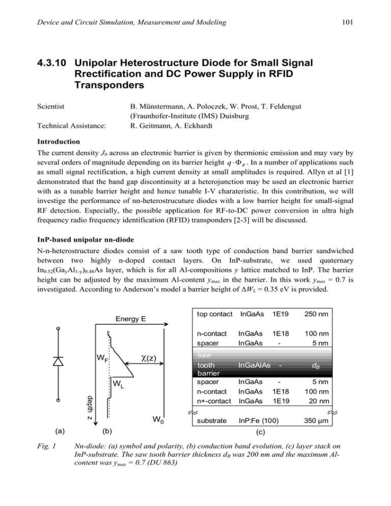
101 Device and Circuit Simulation, Measurement and Modeling 4.3.10 Unipolar Heterostructure Diode for Small Signal Rrectification and DC Power Supply in RFID Transponders Scientist B. Münstermann, A. Poloczek, W. Prost, T. Feldengut (Fraunhofer-Institute (IMS) Duisburg R. Geitmann, A. Eckhardt Technical Assistance: Introduction The current density J0 across an electronic barrier is given by thermionic emission and may vary by several orders of magnitude depending on its barrier height q B . In a number of applications such as small signal rectification, a high current density at small amplitudes is required. Allyn et al [1] demonstrated that the band gap discontinuity at a heterojunction may be used an electronic barrier with as a tunable barrier height and hence tunable I-V charateristic. In this contribution, we will investige the performance of nn-heterostrucuture diodes with a low barrier height for small-signal RF detection. Especially, the possible application for RF-to-DC power conversion in ultra high frequency radio frequency identification (RFID) transponders [2-3] will be discussed. InP-based unipolar nn-diode N-n-heterostructure diodes consist of a saw tooth type of conduction band barrier sandwiched between two highly n-doped contact layers. On InP-substrate, we used quaternary In0.52(GayAl1-y)0.48As layer, which is for all Al-compositions y lattice matched to InP. The barrier height can be adjusted by the maximum Al-content ymax in the barrier. In this work ymax = 0.7 is investigated. According to Anderson’s model a barrier height of ΔWL = 0.35 eV is provided. Energy E (z) WF depth z Fig. 1 W0 (b) InGaAs 1E19 250 nm n-contact spacer InGaAs InGaAs 1E18 - 100 nm 5 nm saw tooth barrier InGaAlAs - dB 1E18 1E19 5 nm 100 nm 20 nm spacer InGaAs n-contact InGaAs n+-contact InGaAs WL (a) top contact substrate InP:Fe (100) 350 µm (c) Nn-diode: (a) symbol and polarity, (b) conduction band evolution, (c) layer stack on InP-substrate. The saw tooth barrier thickness dB was 200 nm and the maximum Alcontent was ymax = 0.7 (DU 863) 102 Bi-Annual Report 2008/2009 - Solid-State Electronics Department The layer stack was grown by molecular beam epitaxy in a Varian GenII apparatus on s. i. InP:Fe substrate (cf. fig. 1c). During growth of the In0.52(GayAl1-y)0.48As barrier (0 < y ≤ 0.7, the Indium cell BEP was kept constant at 3.10-7 Torr. The sum of the Al- and Ga-cell BEP was also kept constant while both, the Ga- and the Al- cell temperature were inversely ramped in order to reach an outmost linear slope of the Al-/Ga-composition within the whole saw tooth barrier. The device processing was done with optical contact lithography, wet chemical etching, and lift-off. A coplanar contact pattern enabling on-wafer RF measurements is used. DC/RF characteristics and Device model The nn-diode I-V characteristic is dominated by the barrier height due to the conduction band discontinuity ΔWL at the In0.52(Al0.7Ga0.3)0.48As/In0.53Ga0.47As heterojunction. The best fit of simulated data to experimental reverse and forward I-V characteristics is obtained for a barrier height of 0.25 eV which is about 0.1 eV less than the nominal data. To analyze the device capacitance a small signal equivalent circuit as shown in fig. 2 was used including the parasitic capacitance Cpad = 20 fF and the inductance Ls = 45 pH. The intrinsic diode is described by the series resistor R and the capacitance C(VD), and the parallel resistance R(VD). The device capacitance C(VD) has been determined by fitting the parameters to the measured rfdata. The extracted values increases from 0.8 fF/µm2 to 1.1 fF/µm2. For a first guess of the switching speed of the device, the speed-index s might be used: (2) s t I V C ps / V . The nn-diode with ymax = 0.7 reached a speed index of s = 50 ps/V at a bias as low as VD = 0.15 V which shows its potential for low-signal microwave applications. Based on the DC and small-signal data a large-signal device model has been developed. The device model is based on a standard pnjunction model included in the “Advanced Design System” software and shows good agreement between measured and modeled DC and RF characteristics (800 MHz to 6 GHz). The scalability of the derived model has been tested on emitter sizes between 16 µm2 and 120 µm2 and can be used to predict the behavior of the needed low capacitance devices for application in RFID-rectifiers. pad VD Fig. 2 RS intrinsic device L S = 45 pH Cpad 20 fF VD,int C(V D) R(V D) Small Signal equivalent model of an InP-based unipolar n-n-heterostructure diode Radio frequency identification transponder In Radio Frequency Identification (RFID) systems the required power for driving the transponder circuits has to be generated by the received RF-signal power. Therefore voltage rectifier circuits are needed to convert the high frequency signal into a stable DC supply voltage [4, 5]. Several stages Device and Circuit Simulation, Measurement and Modeling 103 are implemented in a cascaded charge-pump structure in order to generate sufficient DC voltage for the operation of integrated circuits (cf. fig. 3). The power efficiency and the minimum input voltage requirements of the rectifier determine the maximum distance between the remotely powered device and the base station. For efficient rectification diodes with relatively high switching speed at a low forward bias are required. The investigated nn-heterostrucuture diode exhibits at VD = 0.15 V an ideality factor of n = 1.2, a current density of 20 µA/µm², and a rectification factor of GR = 30. Fig. 3 UHF voltage multiplier/rectifier In fig. 4 a transient simulation of the ac current id(Vd(t)) within the initial 10 µs is compared to the device DC I-V characteristics with 5 µm² emitter area. The observed voltage drop in forward direction is reduced to 150 mV, while in the negative regime the blocking effect is illustrated. The maximum current of 100µA (20µA/µm2) is used to load the following capacitor in the charge-pump architecture. Optimization has shown that a drastic reduction of the emitter size to 5µm2 of the diodes increases Vin and provides a voltage supply of 1.5 V for a minimum received rf-power of 13,6 dBm. Fig. 4 I-V-characteristics and transient diode current of the device in the rectifier circuit. The observed forward voltage drop is 150 mV for a 5 µm2 emitter area device 104 Bi-Annual Report 2008/2009 - Solid-State Electronics Department In tab. 1 the performance of the multistage rectifier using nn-diodes is compared with previous publications based on Si-Schottky diodes. The maximum operating range of the FRID for a basestation which transmits 3.28 W RF power at a carrier frequency of 864 MHz has been calculated. Using the nn-diodes the operating range of the system can be improved by 30%. The conversion efficiency is for the given load conditions is 17%, which is an excellent value compared to the conventional rectifiers. Tab. 1 this work min RF-Power for 1.5 V, 5µA -13,6 dBm max. distance to base station 7,5 m RF to DC efficiency 17 % [10] -10,5 dBm 5,4 m 12 % [11] -11,3 dBm 5,74 m 10 % Performance data of the investigated cascaded charge-pump circuit for remote RFID DC power supply based on nn-diodes in comparison to works using Si-Schottky diodes [10, 11]. Conclusion A unipolar nn-heterostructure diode on InP-substrate is developed with an In0.52(GayAl1-y)0.48As saw tooth barrier layer with 0 < y < 0.7. The electronic transport across the barrier can be described by thermionic emission theory. In this study the device with a low barrier height is investigated for AC-to-DC conversion in remote powered RFID requiring high current densities and high rectification factors at low bias. In comparison to a standard Si-Schottky diode 3 dBm less RFpower is needed while the efficiency increases from 12 % to 17 %. References [1] [2] [3] [4] [5] C. L. Allyn, A. C. Gossard and W. Wiegmann; „New rectifying semiconductor structure by molecular beam epitaxy“, Appl. Phys. Lett. 36(5) 373-375, 1990. U. Karthaus, M. Fischer; “Fully Integrated Passive UHF RFID Transponder IC With 16.7µW Minimum RF Input Power”; IEEE J Sol.-State Circ.. vol. 38, no. 10, 2003. R. E. Barnett, J. Liu, S. Lazar; A RF to DC Voltage Conversion Model for Multi-Stage Rectifiers in UHF RFID Transponders, IEEE J. Sol.-State Circ.. vol. 44, no. 2, 2009. J.-P. Curty, N. Joehl, C. Dehollain, and M. J. Declercq; “Remotely Powered Addressable UHF RFID Integrated System”, IEEE Sol.-State Circ. Vol. 40, no. 11, p. 2193, 2005. T. Feldengut, R. Kokozinski, S. Kolnsberg; “A UHF Voltage Multiplier Circuit Using a Threshold-Voltage Cancellation Technique”, PRIME Conf. Proc., p.288-291 July 2009.


