Lab 5: Creating bonding pads
advertisement

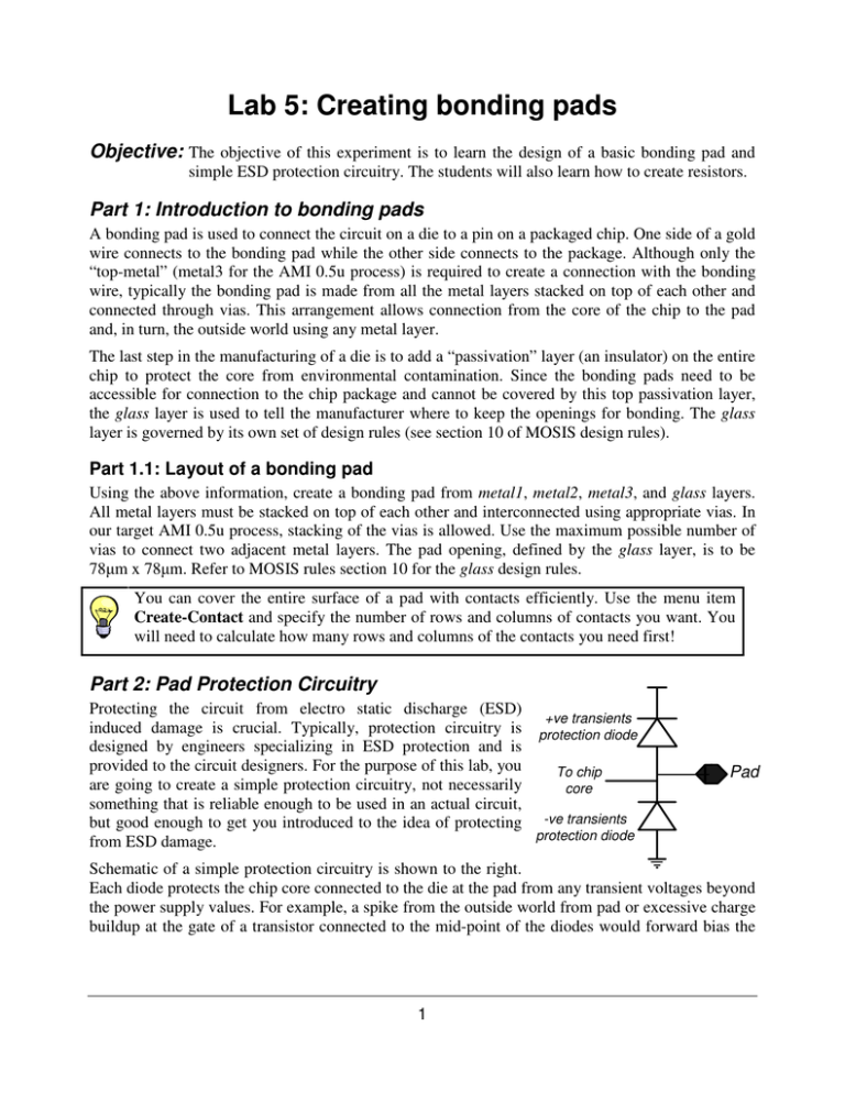
Lab 5: Creating bonding pads Objective: The objective of this experiment is to learn the design of a basic bonding pad and simple ESD protection circuitry. The students will also learn how to create resistors. Part 1: Introduction to bonding pads A bonding pad is used to connect the circuit on a die to a pin on a packaged chip. One side of a gold wire connects to the bonding pad while the other side connects to the package. Although only the “top-metal” (metal3 for the AMI 0.5u process) is required to create a connection with the bonding wire, typically the bonding pad is made from all the metal layers stacked on top of each other and connected through vias. This arrangement allows connection from the core of the chip to the pad and, in turn, the outside world using any metal layer. The last step in the manufacturing of a die is to add a “passivation” layer (an insulator) on the entire chip to protect the core from environmental contamination. Since the bonding pads need to be accessible for connection to the chip package and cannot be covered by this top passivation layer, the glass layer is used to tell the manufacturer where to keep the openings for bonding. The glass layer is governed by its own set of design rules (see section 10 of MOSIS design rules). Part 1.1: Layout of a bonding pad Using the above information, create a bonding pad from metal1, metal2, metal3, and glass layers. All metal layers must be stacked on top of each other and interconnected using appropriate vias. In our target AMI 0.5u process, stacking of the vias is allowed. Use the maximum possible number of vias to connect two adjacent metal layers. The pad opening, defined by the glass layer, is to be 78 m x 78 m. Refer to MOSIS rules section 10 for the glass design rules. You can cover the entire surface of a pad with contacts efficiently. Use the menu item Create-Contact and specify the number of rows and columns of contacts you want. You will need to calculate how many rows and columns of the contacts you need first! Part 2: Pad Protection Circuitry Protecting the circuit from electro static discharge (ESD) +ve transients induced damage is crucial. Typically, protection circuitry is protection diode designed by engineers specializing in ESD protection and is provided to the circuit designers. For the purpose of this lab, you To chip are going to create a simple protection circuitry, not necessarily core something that is reliable enough to be used in an actual circuit, but good enough to get you introduced to the idea of protecting -ve transients protection diode from ESD damage. Pad Schematic of a simple protection circuitry is shown to the right. Each diode protects the chip core connected to the die at the pad from any transient voltages beyond the power supply values. For example, a spike from the outside world from pad or excessive charge buildup at the gate of a transistor connected to the mid-point of the diodes would forward bias the 1 CprE/EE434 Lab 5: Creating bonding pads top diode. Consequently, the diode will conduct and protect the core of the chip from getting damaged. Part 2.1: Schematic of the ESD protection circuit Create a new cell (you may call it bondingPadWithESD or something similar) and enter the schematic of ESD circuitry described previously (the Pad is just a pin). This schematic will be used for LVS later. Part 2.2: Layout of a diode Diodes can be created two ways: p+ and n+ diffusions inside either an n-well or the substrate. For the purpose of this lab, we will layout each diode in its own n-well. For extraction to work correctly, you have to completely cover the two adjacent diffusions with the layer dio_id, For this lab, the total area occupied by the protection circuit (both diodes) will be equal to the total area of the bonding pad itself. With this in mind, create the layout of one diode in a cell by itself and make sure that it extracts as a diode. We will ignore the electrical properties of this diode and focus only on the correct connectivity. Part 2.3: Layout of the complete bonding pad With a layout of a single diode and a bonding pad available, you will now create a layout of bonding pad with ESD protection. Create a layout view of the cell bondingPadWithESD, instantiate the needed components, and complete the bonding pad design. Make sure you pass LVS. This complete bonding pad will be used later in the lab. Part 3: Layout of a resistor The next step is to learn how to create a resistor. A resistor can be created using almost any layer available in the process. For example, to create a resistor using poly, draw a poly with terminals at its ends as shown below (poly is red, metal1 is blue, and cyan is res_id). For correct extraction of these “intended” resistors, you need to cover the poly with the identification layer called res_id. From its name, we can deduce that this is an identification layer, not an actual physical layer for fabrication. The number of squares of poly covered by the res_id layer are used to calculate the value of the resistance. The res_id layer must be used to create resistors in all possible layers (listed in a table on the next page) except for the high_res layer. The high_res (high resistance) layer, in contrast with res_id, is a physical layer i.e., sent to foundry but does not correspond to actual physical shape. When used with the poly2(elec for our environment) layer, the high_res layer results in increased resistance of 2 CprE/EE434 Lab 5: Creating bonding pads poly2 (elec) layer. If you intend to use the high_res layer, follow the design rules on MOSIS website (see section 27). The following table provides the sheet resistance of all the layers that can be used to create resistors for the AMI 0.5u process. Layer Sheet resistance per square nwell 819 poly 25 elec (poly2) 26 metal1 0.090000 metal3 0.050000 metal2 0.090000 highres 1192 You are to create a resistor of value approximately 5 K while minimizing the area of the resistor. You can ignore the resistance of the contacts for the purpose of this lab. 3

