HIGH SPEED POWER AMPLIFIER
advertisement
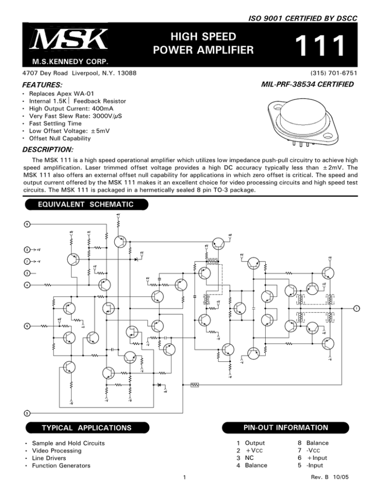
ISO 9001 CERTIFIED BY DSCC HIGH SPEED POWER AMPLIFIER 111 M.S.KENNEDY CORP. 4707 Dey Road Liverpool, N.Y. 13088 (315) 701-6751 MIL-PRF-38534 CERTIFIED FEATURES: Replaces Apex WA-01 Internal 1.5KΩ Feedback Resistor High Output Current: 400mA Very Fast Slew Rate: 3000V/µS Fast Settling Time Low Offset Voltage: ±5mV Offset Null Capability DESCRIPTION: The MSK 111 is a high speed operational amplifier which utilizes low impedance push-pull circuitry to achieve high speed amplification. Laser trimmed offset voltage provides a high DC accuracy typically less than ±2mV. The MSK 111 also offers an external offset null capability for applications in which zero offset is critical. The speed and output current offered by the MSK 111 makes it an excellent choice for video processing circuits and high speed test circuits. The MSK 111 is packaged in a hermetically sealed 8 pin TO-3 package. EQUIVALENT SCHEMATIC PIN-OUT INFORMATION TYPICAL APPLICATIONS 1 2 3 4 Sample and Hold Circuits Video Processing Line Drivers Function Generators 1 Output +VCC NC Balance 8 7 6 5 Balance -VCC +Input -Input Rev. B 10/05 7 ABSOLUTE MAXIMUM RATINGS Total Supply Voltage Output Current Differential Input Voltage Common Mode Input Voltage VCC IOUT VIN VIN ○ ○ ○ ○ ○ ○ ○ ○ ○ ○ ○ ○ ○ ○ ○ ○ ○ ○ ○ ○ ○ ○ ○ ○ ○ ○ ○ ○ ○ ○ 32V 0.4A ±6V ±VCC ○ ○ TST TLD ○ ○ TC Storage Temperature Range Lead Temperature Range (10 Seconds) Case Operating Temperature MSK111 MSK111H/E Junction Temperature ○ ○ ○ ○ ○ ○ ○ TJ ○ ○ ○ ○ ○ ○ ○ ○ ○ ○ ○ ○ ○ ○ ○ ○ ○ ○ ○ ○ ○ ○ ○ ○ ○ ○ ○ ○ ○ ○ ○ ○ ○ ○ -65°C to +150°C 300°C ○ ○ ○ ○ ○ ○ ○ -40°C to +85°C -55°C to +125°C 175°C ○ ○ ○ ○ ○ ○ ○ ○ ELECTRICAL SPECIFICATIONS Group A Parameter MSK 111H/E Test Conditions 1 MSK 111 Units Subgroup Min. Typ. Max. Min. Typ. Max. - ±12 ±15 ±16 ±12 ±15 ±16 V 1 - ±28 ±30 - ±28 ±35 mA 2,3 - - ±50 - - - mA 1 - ±0.5 ±5 - ±0.5 ±10 mV 2,3 - - ±30 - - - mV STATIC Supply Voltge Range 2 Quiescent Current VIN=0V INPUT Input Offset Voltage VIN=0V 2 Input Bias Current 1 - 5 20 - 5 30 µA VCM=±5V 4 48 54 - 48 54 - dB VCC=24V to 30V 1 60 75 - 60 75 - dB Output Voltage Swing f=1KHz RL=1KΩ 4 ±10 ±11 - ±10 ±11 - V Output Current f=1KHz RL=50Ω 4 400 - - 400 - - mA Power Bandwidth 2 VO=20VPP - - 40 - - 40 - MHz Settling Time 2 10V Step - - 20 - - 20 - nS VOUT=±10V RL=1KΩ 4 2500 3000 - - V/µS T C =25°C - - 2.9 - - 2.9 - nS Junction to Case @ 125°C - - 31 - - 35 - °C/W Rf - 1.497 1.5 1.5 1.505 KΩ Common Mode Rejection 2 Power Supply Rejection 2 OUTPUT Slew Rate Propagation Delay 2 Thermal Resistance 2 Internal Feedback Resistor 1.503 1.495 NOTES: 1 Unless otherwise specified, ±VCC=±15V AV=10V/V and RL=∞ and Tc=25°C. 2 Guaranteed by design but not tested. Typical parameters are representative of actual device performance but are for reference only. 3 Industrial grade and "E" suffix devices shall be tested to subgroups 1 and 4 unless otherwise specified. 4 Military grade devices ("H" suffix) shall be 100% tested to subgroups 1,2,3 and 4. 5 Subgroup 5 and 6 testing available upon request. 6 Subgroup 1,4 TA=TC=+25°C Subgroup 2,5 TA=TC=+125°C Subgroup 3,6 TA=TC=-55°C 7 Continuous operation at or above absolute maximum ratings may adversely effect the device performance and/or life cycle. 2 2500 3000 30 Rev. B 10/05 APPLICATION NOTES POWER SUPPLY BYPASSING HEAT SINKING Both the negative and the positive supplies must be effectively decoupled with a high and low frequency bypass circuit to avoid power supply induced oscillation. An effective decoupling scheme consists of a 0.01 microfarad ceramic capacitor in parallel with a 4.7 microfarad tantalum capacitor from each power supply pin to ground. All power supply decoupling capacitors should be placed as close to the package power supply pins as possible. Output, power supply, and bypass leads should be kept as short as possible. Long connections can add significant inductance, raising impedance and limiting output current slew rate. This is especially true in the video frequency range. The case of the MSK 111 is electrically isolated and should be connected to a common ground plane. In addition to the case, the input signal and input resistors should be connected to this common ground plane using a single point grounding scheme. This will help to prevent undesired current feedback that can cause instability in the circuit. To select the correct heat sink for your application, refer to the thermal model and governing equation below. Governing Equation: GAIN TJ = PD x (RθJC + RθCS + RθSA) + TA The MSK 111, unlike most operational amplifiers, has an internal feedback resistor. The value of this resistor is 1.5KΩ. Fewer external components are required to configure the MSK 111 in either inverting or non-inverting modes. Using an internal feedback resistor shortens the feedback path, lowering summing node capacitance to ground and stabilizing high frequency characteristics. OUTPUT OFFSET NULL Typically,the MSK 111 has an input offset voltage of less than ±2mV. The input offset voltage is laser trimmed to less than ±5mV, but in applications where offset is critical, the balance pins may be used to null the offset to zero. A 20KΩ potentiometer may be placed between pins 4 and 8 with the wiper arm connected to +VCC. If the balance function is not used pins 4 and 8 should not be connected (floating). However, if settling time is extremely important, pin 8 should be tied to the AC ground with a 100-150pF capacitor. SAFE OPERATING AREA-POWER DISSIPATION The safe operating area curve is a graphical representation of the power handling capability of the amplifier under various conditions. The wire bond current carrying capability, transistor junction temperature and secondary breakdown limitations are all incorporated into the safe operating area curves. All applications should be checked against the S.O.A. curves to ensure high M.T.B.F. Thermal Model: Where TJ PD RθJC RθCS RθSA TC TA TS = = = = = = = = Junction Temperature Total Power Dissipation Junction to Case Thermal Resistance Case to Heat Sink Thermal Resistance Heat Sink to Ambient Thermal Resistance Case Temperature Ambient Temperature Sink Temperature IN Example: In our example the amplifier application requires the output to drive a 10 volt peak sine wave across a 50 ohm load for 0.2 amp of output current. For a worst case analysis we will treat the 0.2 amp peak output current as a D.C. output current. The power supplies are ±15 VDC. 1.) Find Power Dissipation PD=[(quiescent current) x (+VCC - (VCC))] + [(VS - VO) x IOUT] =(28 mA) x (30V) + (5V) x (0.2A) =0.84W + 1W =1.84W 2.) For conservative design, set TJ = +150°C. 3.) For this example, worst case TA = +25°C. 4.) RθJC = 31°C/W 5.) Rearrange governing equation to solve for RθSA: RθSA = (TJ - TA) / PD - (RθJC) - (RθCS) = (150°C - 25°C) / 1.84W - (31°C/W) - (0.15°C/W) = 36°C/W The heat sink in this example must have a thermal resistance of no more than 36°C/W to maintain a junction temperature of less than +150°C. This calculation assumes a case to sink thermal resistance of 0.15°C/W. 3 Rev. B 10/05 TYPICAL PERFORMANCE CURVES 4 Rev. B 10/05 MECHANICAL SPECIFICATIONS CONTAINS INTERNAL BeO (BERYLLIUM OXIDE) WEIGHT = 15 GRAMS TYPICAL NOTE: ALL DIMENSIONS ARE ±0.010 INCHES UNLESS OTHERWISE LABELED ORDERING INFORMATION Part Number Screening Level MSK111 Industrial MSK111E EXTENDED RELIABILITY MSK111H MIL-PRF-38534 CLASS H M.S. Kennedy Corp. 4707 Dey Road, Liverpool, New York 13088 Phone (315) 701-6751 FAX (315) 701-6752 www.mskennedy.com The information contained herein is believed to be accurate at the time of printing. MSK reserves the right to make changes to its products or specifications without notice, however, and assumes no liability for the use of its products. Please visit our website for the most recent revision of this datasheet. 5 Rev. B 10/05
