Electronic Manufacturing Services - Aeroflex Microelectronic Solutions
advertisement
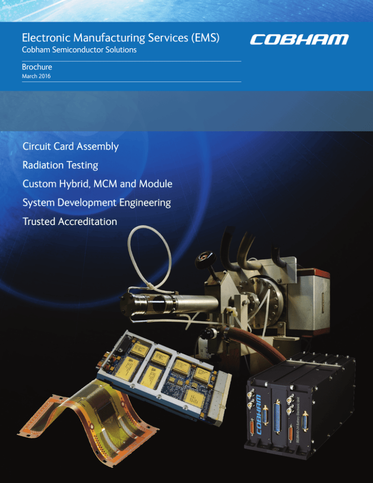
Electronic Manufacturing Services (EMS) Cobham Semiconductor Solutions Brochure March 2016 Circuit Card Assembly Radiation Testing Custom Hybrid, MCM and Module System Development Engineering Trusted Accreditation Cobham Circuit Card Assembly (CCA) Cobham Semiconductor Solutions (formerly Aeroflex) Circuit Card Assembly offers a full turnkey electronic manufacturing operation, including assemblies, modules, and systems complete with testing and coating capabilities, in a domestic facility. We support both consigned and turn-key procurement of customer Bills of Materials, qualify components where necessary, and Build-to-Spec all volumes of boards. Cobham recently completed their Ceramic Column Grid Array (CGA) package qualification with the assistance of Six Sigma Services. Manufacturing Leadership n Assembly processes for both ANSI-J-STD-001 including latest Space Addendum and NASA 8739 n ISO 9001:2008 certified with AS9100:2004 Rev C value‑added compliance n ESD Certified to ANSI-ESD S20.20 for assemblies and Integrated Circuits n Environmental and quality control systems. Colorado “Gold” award winner n Full ITAR compliance Our Automated Circuit Card Assembly line debuted in Fall 2014 – please see video at www.cobham.com/EMS. MyData MY100-4 CCA Automated Line Cobham Circuit Card Assembly (CCA) Manufacturing Support Processes Manufacturing Expertise n Turnkey or consigned manufacturing n Automated surface mount and Plated throughhole assembly – Counterfeit Parts Control Program n Qualified Ceramic Column Grid Array (CGA) assembly – Obsolescence and EOL parts management – Parts management to customer provided requirements (AVL, PAPL, PAMPL) n Automated Optical Inspection (AOI), Solder Paste Integrity measurements (SPI) and Coordinate Measuring (CMM) for critical dimension measurements. – Component traceability by Lot Date Code or customer provided tracking process n Incoming XRF screening for all Military and Space programs (pure tin and speciality metal detection) n 2D 360 degree rotational Real Time Xray n Burn-in capabilities at assembly, module and box level n Component lead forming, part programming and post-delivery component level test screening as part of the assembly services n Flying Probe n System Level Board testing capable n Shock, Vibration and Temperature nConformal Coating to Mil-I46058 standards My Data Flying Probe Board Router FARO Aeroflex Colorado Springs and Plainview – Category 1A Trusted Accreditation by DMEA PARMI Radiation Testing Qualification Services MIL-STD Radiation Effects Test Services n Total Ionizing Dose (TID) RLAT (50 to 300 rads/sec) – MIL-STD-883 Test Methods 1019, Cond. A n TID ELDRS (10 to 100 mrads/sec) Quick-Turn Prototype IC Assembly Cobham RAD offers the following services: Quick-Turn Prototype IC Assembly in ceramic, etched out plastic, COB and flip chip. – MIL-STD-883 Test Methods 1019, Cond. D, Quick-Turn Prototype IC Assembly Capabilities ESA/SCC22900 n Dicing, Die Visual and Die Attach n Prompt Dose / Flash X-Ray Tests – Wafer Dicing (up to 12inch wafers) – MIL-STD-883 Test Methods 1020 and 1021 n Neutron Displacement Damage Tests n Heavy Ion SEE Tests (SEL, SET, SEGR, SEU, SEB, SEFI) – Visual Inspection (50-500X) – Conductive and non-conductive epoxy die attach – Silver Glass and Eutectic die attach n Proton SEE and Displacement Damage Tests – Flip Chip n Cryogenic Focal Plane Array testing (25 K) n Wirebond, Encapsulation and Marking – Gold and Aluminum Wirebond (to 35μm pitch) Device Preparation for Single Event Effects Testing Preparation for Single Event Effects (SEE) Testing can be quite demanding. Cobham RAD can significantly lessen these demands by using Cobham RAD proprietary processes and techniques that simplify this task. Backside thinning to 35μm allows for SEE Testing at TAMU or Berkeley without repackaging of ICs. Finished Package Backside Thinning n Package backside thinning to 35μm ±5μm n Custom PC board design in preparation for SEE Testing n Custom DUT Socket Solutions for SEE Testing of multiple interchangeable ICs for at-speed testing on a test board Die Thinning n Die thinning is available as required to any thickness (±5μm) Die Extraction / Repackaging n When package backside thinning is not a solution, we routinely perform die extraction and repackaging in preparation for SEE Testing n Custom PC board design for SEE Testing is available – Epoxy, Solder, and Glass Frit Lid Seal – Dam and Fill (Plastic Encapsulation) • Plastic Equivalent Devices • COB Glob Top – Package Ink Marking or Laser Marking n Package Options – Multi-chip / Stacked Modules, Chip-On-Board (COB), and Custom Substrates – Ceramic Packages Including: BGA, PGA, J-Lead, Flat Pack, QFP, Sidebraze, CERDIP and others – Etched Cavity Plastic Packages Including: J-Lead, QFP, SOIC, TSSOP, QFN /MLF and others Specialty Services Systems Development Engineering Cobham SDE enables customers to focus on their core competencies n System Development Engineering • • • • Single Board Computing Custom Filter and Hybrid Power Converter Modules Battery Management Units NYQUIST Filter Switched Filter Module n Electronic Manufacturing Services • • RAD and Other Test Screening Services Circuit Card, Module and Unit Assembly and Test n ASIC Products and Design • • Industrial and Aerospace Security and Medical Lumped Element Filters n Standard Products • • ADC/DAC, Muxes, Op Amps, PWMs, Voltage Regulators Microprocessors, Memories, Interconnect (Logic and Clock) GEN6 SBC Packaging Cobham Semiconductor Solutions has developed the capability of Custom Packaging along with the commercially available plastic packaging n Package Technology Overview •Commercial Plastic Packages: BGA and fpBGA (81 to 484 pin), QFN (12 to 64 pin), PQFP (40 to 208 pin), in pitches ranging from 1.27 to 0.4mm •HiRel Packages: Hermetic ceramic package technology, from 12 to 377 user I/O; CQFP, CCGA, LGA, PGA, DFP •QML-V certification per MIL-PRF-38535 •Class Y facility certification per MIL-PRF-38535; first Class Y certification awarded by DLA •QML qualified chip cap attach and solder column attach processes n Plug & SenseSM Packaging Examples • • • • Flip-Chip on Flex, Organic, or Ceramic assembly Stacked Sensor to ASIC design 4,096 Channel Bio-Sensor with 2 ASICs Two 512 Channel Flip-Chip ASICs plus Flip-Chip Bio Sensor n Advanced Package Technology • • • • • • Stacked Die assembly MRAM magnetic shielding assembly Advanced Flip-Chip assembly (Class Y) Decoupling Capacitor attach to package (Class Y) Heat Sink attach (Class Y) Seam Seal and Laser Mark Electronic Manufacturing Services (EMS) Cobham Semiconductor Solutions Cobham Custom Hybrid, MCM and Module Services Cobham, a supplier of standard products and custom microelectronic solutions offers Space and Military qualified assembly and test services meeting the requirements of MIL‑PRF-38534 Class H & K. Our MCM packaging technology enables our customers to realize the optimum Size, Weight and Power (SWaP) of their products by applying flip-chip, chip and wire, Chip-on-Board (COB), Surface Mount Technology (SMT) and Planar Magnetics. In many cases, more than one of these technologies are combined in a single module. n RF/microwave manufacturing services for high volume phased array antennas n Value-added services such as radiation testing and characterization, classified testing and COTS/commercial upscreening n Cobham HiRel products, such as FPGAs and ASICs, are available for vertical integration From DC to 40 GHz, Cobham can provide microelectronic packaging and test solutions for high speed digital, precision analog and RF/Microwave devices used in military, space and critical industrial applications. Cobham Offers n One stop solution for your microelectronic assembly, evaluation, test and screening requirements Production Capabilities n MIL‑PRF‑38534 compliant (Class H & K), ISO‑9001 and AS9100 certified n State-of-the-Art gold ball bonding: n Customer furnished tooling - Cobham is experienced in integrating customer originated designs into a smooth, seamless high quality process – 0.8 mil to 2.0 mil automatic gold ball bonding – Typical IC bond pad dimensions: 65µm; 50µm on special request n Full turnkey and "design to spec" services for hybrid, SMT assemblies and boxes – Typical IC bond pad pitch: 80µm; 75µm on special request n Vertically integrated die to box facility, Class 1,000, Class 10,000 and Class 100,000 manufacturing space – Standard operating procedure: Security Bump on Stitch n High-reliability Chip‑On‑Board design and manufacturing services – Specialized stand-off stitch allows inter-chip, highspeed ball bonding versus slower wedge bond processes – Large Area – 16” x 13” bondable area The most important thing we build is trust. www.cobham.com WEB SITESEMS www.cobham.com/EMS HiRelwww.cobham.com/HiRel RADwww.cobham.com/rad Cobham Semiconductor Solutions Part No, EMS – 3-2016 TELEPHONE ©2016 COBHAM 1-800-645-8862
