PNP or NPN. - Computer History Museum
advertisement
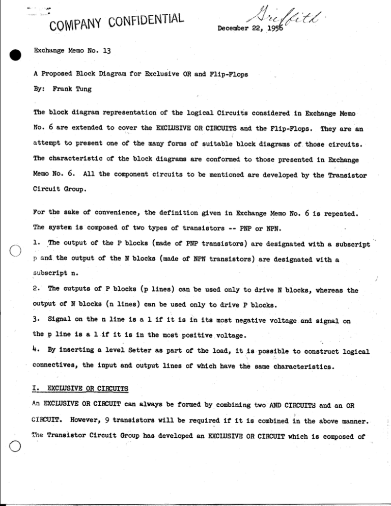
December 22, 1956' Exchange Elemo No. 13 A Proposed Block Diagram for Exclusive OR and Flip-Flops Frank Tung By: The block diagram representation of the logical Circuits considered in Exchange Memo No. 6 are extended to cover the EXCLUSIVE OR CIRCUITS and the Flip-Flopo. They are an attempt to present one of the many forms of suitable block diagrams o f those circuits. The characteristic of the block diagrams are conformed to those presented In &change Memo No. 6. All the component circuits to be mentioned are developed by the Transistor Circuit Group. For the sake of convenience, the definition given in Exchange Memo No. 6 is repeated. The system is composed of two types of transistors 0 0 - PNP or NPN. 1. ,The output of the P blocks (made of PNP transistors) are designated with a subscript p and the output of the N blocks (made o f NPN transistors) are designated with a aubscript n. / 2. The outputs of P blocks (p lines) can be used only to drive N blocks, whereas the output of N blocks (n lines) can be used only to drive P blocks. 3. Signal on the n line is a 1 if I t is in its most negative voltage and signal on %he p line is a 1 if it is in the most positive voltage. 4. By inserting a level Setter as part of the load, it is possible to construct logical connectives, the input and output lines of which have the same characteristics. 11 E X C U S N E OR CIXUITS An EXCLUSIVE CTXUIT. OR CIXUIT can always be formed by combining two AND CIRCUITY and an OR i However, 9 transistors will be required if it is combined in the above manner. The Transistor Circuit Group has developed an EXCLUSIVE OR CIRCUIT which is composed of 0 --em" Exchange Memo No. 13 0 either 6 transistors or 4 transistors. December 22, 1956 The 4 transistor EXCLUSIVE OR CIRCUIT offers no complemented output. One of the applications where an EXCLUSIVE OR connective would prove extremely useful in the Exchange lies in the operation of stepping the word count -1 and the Data word address+l. By using an EXCLUSIVE OR and an AND connectives for each bit, the carry propagation time is determined solely by the number of parallel blocks that can be cascaded at an output of a logical connective and the number of parallel inputs %hat a logical connective can handle. a. The circuit and the corresponding block diagram of a 6 PNP transistor EXCLUSIVE OR connective with complemented outputs are shown in Figure 1. By reversing the subscripts, the same block diagram can be used for the NPN version of the same circuit. 0 Only two lines are shown leading to the input of the block. The actual circuit involves the connection up to four inputs -- the two signals and the complements of A block diagram that m y be used to represent a each signal. 4 transistor EXCLUSIVE OR connective which has no complementary outputs is shown in Figure 2. The actual circuits has only two inputs as those shown. 0 , Figure 2 Exchange Memo No. 13 --3-- December 22, 1956 The saving of the two t r a n s i s t o r s is a t the expanse of adding 4 diodes and two current sources. Each current source supplies the amount equals t o the d.c. current of the conducting t r a n s i s t o r . II. FLIP-FLOPS A. Standard Flip-Flops The state of the standard Flip-Flop is determined by the application of a pulse at e i t h e r t h e Set o r Reset terminals. The p o l a r i t y of the pulse depends on the type of t r a n s i s t o r s that made up the Flip-Flop. The input terminals a r e normally a t the voltage which corresponds t o a zero f o r the p a r t i c u l a r l i n e . For instance, the input signal w i l l be a t i t ' s most positive voltage if it is an n l i n e , the Flip-Flop the input signal is changed t o its 1 state. I n order t o t r i g g e r Depending on the type of input l i n e s , t h i s change may appear either as a positive o r a negative pulse. Two d i f f e r e n t types of Standard Flip-Flops w i l l be considered. l o Flip-Flop composed of both NPN and PNP type tranoistors. 2. Flip-Flop composed of either the NPN o r t h e PNP type t r a n s i s t o r s . 1. Figure 3 shows t h e c i r c u i t configuration and the block diagram representation o f a standard Flip-Flop incorporating both type of t r a n s i s t o r s . The features of t h i s c i r c u i t and the notations are explained as follows: a. The basic c i r c u i t with no input t r i g g e r c i r c u i t s requires 4 t r a n s i s t o r s . b, It has both types of outputs (p l i n e and n l i n e s ) and t h e i r complements. c. K is the number of p a r a l l e l input t r a n s i s t o r s shown dotted i n Figure 3. The maximum possible number of K is t o be determihed by the Circuit Group. p a r a l l e l connection of those input t r a n s i s t o r s serves as an OR function. since it is specified by the number of incoming arrow8. The K is redundant However, it may simplify the Exchange Memo No. 13 0 -*4-- December 22, 1956 packaging problem if the Flip-Flops are t o be mass produced as separate pluggable units. d. The state of the Flip-Flop i s conditioned as follows: 1. Dn = inputs (zip -Dn= 2. \ 1, Dpm 1 Upon application of a 1 a t e i t h e r of the K p l i n e 9 1, 5 P inputs (xln, ------ ,'kp) =1 Upon application of a 1 at e i t h e r of the K n l i n e ------ 9Xkn) e. The'complernent of the signal i s denoted with a bar. f. The subscript p and n on the output terminals may be removed i f I t is remembered t h a t the l e f t side gives a p l i n e output and the r i g h t s i d e gives a n line output which can be differentrated by the positions of the subscript associated with the i n i t i a l s F.F. g. 0 The p a r t i c u l a r arrangement of the block diagram, i s that t h e top l e f t output is a 1 if' It i s triggered from the l e f t and the top r i g h t output is a 1 i f It I s triggered from the r i g h t . c Figure 3 &change Memo No. 13 December 22, 1956 --$-- Another block diagram representation of a Standard Flip-Flop whose c i r c u i t configuration is shown i n Figure 3, has been s u g p s t e d . It resembles the one j u s t proposed. It is shcwn i n Figure 3a. Figure 3a The * fo m o f t h i s representation i s such that: 1. The o v e r a l l block diagram i s reduced t o three simplified blocks each one of which can be easily grasped. 2. Logic-wise, only one new block i s introduced. 3. The two small blocks perform the function of a (The Flip-Flop) OR c i r c u i t f o r the inputs. The bo sign s i g n i f i e s t h a t OR block i s a c t u a l l y p a r t of the Flip-Flop. 4. The number of inputs is specified by the number of arrows leading i n t o the OR block. Figure 4 shows t h e block diagram used by the c i r c u i t group of t h e Exchange t o represent a Standard Flip-Flop t h a t has two input terminals type o f t r a n s i s t o r used. -- OFF and ON. It i s included here f o r reference. P and N stand f o r the -&- Exchange Memo No. 13 2. December 22, 1956 ' The Standard Flip-Flop composed of either the PNP o r the NPN type t r a n s i s t o r s has been developed. It involves the use of selenium diodes and extra power supplies as the l e v e l setter a t the collector c i r c u i t . n lines. Both the inputs and the outputs are The block diagram representation and the component c i r c u i t of a Standard Flip-Flop of t h e PNP type i s shown i n Figure 5. The state of the Flip-Flop i s determined by the application of a negative pulse o r a 1 a t e i t h e r one of the many Set o r Reset input terminals. R denotes the number of inputs which i s the number of t r a n s i s t o r s connected i n parallel as shown dotted, The Flip-Flop i t s e l f requires 4 t r a n s i s t o r s , The input terminals are normally a t a voltage which corresponds t o a 0. If a two l e v e l logic system is adopted, kll the subscripts can be omitted, except one, I since the d i f f e r e n t r a t i o n between the n l i n e and the p l i n e is no longer necessary. !Chis subscript i s used only t o indicate the type of t r a n s i s t o r used. 0 Figure 5 The c i r c u i t of Figure 5 also applies t o NPN type t r a n s i s t o r s by reversing the p o l a r i t i e s of the selenium r e c t i f i e r s and the power supplies, 0 reverse t h e p o l a r i t i e s of the input t r i g g e r pulses. It, however, 8180 becomes necessary t o If the most negative of t h e two I s considered 8s a 1, it results t h a t a change from a 0 t o 1w i l l be required t o -..7-- Exchange Memo No. 13 December 22, 1956 t r i g g e r a PNP type Flip-Flop whereas a change from a 1t o 0 w i l l be required t o t r i g g e r a NPN type Flip-Flop. If. BINARY FLIP-FLOP A Binary Flip-Flop changes i t s state upon the application of 'a pulse at the binary input terminal. Many binary Flip-Flop Circuits have been developed by the Transistor C i r c u i t Group. New c i r c u i t s are s t i l l being investigated, Like the standard Flip- Flop it is conceivable that a number of t r a n s i s t o r s may be paralleled as input terminals that perform an OR function. The block diagram of a binary f l i p - f l o p made of one type of t r a n s i s t o r t h a t has two complementary outputs i s shown i n Figure 6. Figure 6 h e notationxis as follows: a. BFF stands f o r binary Flip-Flop. b. Subscript n stands f o r the type of t r a n s i s t o r (PNl?), the type of input l i n e s (n l i n e ) and the type of output l i n e s (n lines.) c. K denotes t h e number of inputs. Each one of which may be used t o t r i g g e r the 113. CONCLUSION Certain l o g i c a l consequence can be inferred from the study of the block diagram 4 Exchange Ekmo No. 13 December 22, 1956 -&- representation with respect to the mzny developed circuits. Some of the obvious points which deserve consideration arc as follows: 1, The degree of couplicatlon introduced by EL four level logic in a large system. 2. The accessibility of both type of tramistors. 3. The reliability of the selenium rectifiers. 4. By using both type of transistors and two level logic, the advantages are: a. Block diagram-wise the symbols shown going into a block are the actual wiring lay out. b. No restriction on the type of transistors to be cascaded. C. Complemented outputs are not essential. Therefore, only one selenium rectifier is necessary per logical block. Whereas the disadvantages are: a. A saving of transistors m y be derived from using a four level logic, b, Extra power supplies are neceseary for the Level Setter. To be specific, a t the present operating point of the Junc$ion Alloy Transistor ( 4 m a ) an extra 8 ma at about 40 volts is necessary per output terminal, The choice of adopting a standard number of circuits for the computer depends upon many other factors, No evaluation has been attempted here, The decision should be reached from the basis which can best be arrived at from an extenaive study of laying out a complicated overall logical system, using different types of block diagrams, After a decision ie made, the notation o f the block diagram may further be simplified. Some redundant subscripts may not be necessary. Efforts will be spent toward this direction,
