Welding Machines Converters Using TRENCHSTOP™ 5
advertisement

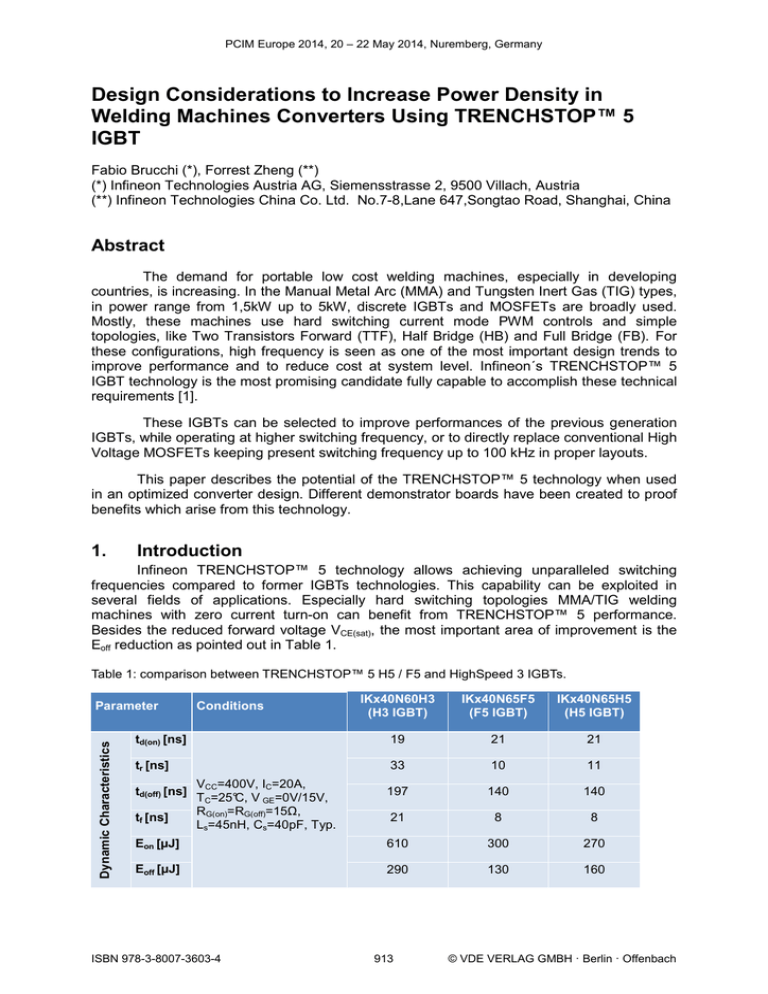
PCIM Europe 2014, 20 – 22 May 2014, Nuremberg, Germany Design Considerations to Increase Power Density in Welding Machines Converters Using TRENCHSTOP™ 5 IGBT Fabio Brucchi (*), Forrest Zheng (**) (*) Infineon Technologies Austria AG, Siemensstrasse 2, 9500 Villach, Austria (**) Infineon Technologies China Co. Ltd. No.7-8,Lane 647,Songtao Road, Shanghai, China Abstract The demand for portable low cost welding machines, especially in developing countries, is increasing. In the Manual Metal Arc (MMA) and Tungsten Inert Gas (TIG) types, in power range from 1,5kW up to 5kW, discrete IGBTs and MOSFETs are broadly used. Mostly, these machines use hard switching current mode PWM controls and simple topologies, like Two Transistors Forward (TTF), Half Bridge (HB) and Full Bridge (FB). For these configurations, high frequency is seen as one of the most important design trends to improve performance and to reduce cost at system level. Infineon´s TRENCHSTOP™ 5 IGBT technology is the most promising candidate fully capable to accomplish these technical requirements [1]. These IGBTs can be selected to improve performances of the previous generation IGBTs, while operating at higher switching frequency, or to directly replace conventional High Voltage MOSFETs keeping present switching frequency up to 100 kHz in proper layouts. This paper describes the potential of the TRENCHSTOP™ 5 technology when used in an optimized converter design. Different demonstrator boards have been created to proof benefits which arise from this technology. 1. Introduction Infineon TRENCHSTOP™ 5 technology allows achieving unparalleled switching frequencies compared to former IGBTs technologies. This capability can be exploited in several fields of applications. Especially hard switching topologies MMA/TIG welding machines with zero current turn-on can benefit from TRENCHSTOP™ 5 performance. Besides the reduced forward voltage VCE(sat), the most important area of improvement is the Eoff reduction as pointed out in Table 1. Table 1: comparison between TRENCHSTOP™ 5 H5 / F5 and HighSpeed 3 IGBTs. IKx40N60H3 (H3 IGBT) IKx40N65F5 (F5 IGBT) IKx40N65H5 (H5 IGBT) td(on) [ns] 19 21 21 tr [ns] 33 10 11 197 140 140 21 8 8 Eon [µJ] 610 300 270 Eoff [µJ] 290 130 160 Dynamic Characteristics Parameter Conditions V =400V, IC=20A, td(off) [ns] CC TC=25°C, V GE=0V/15V, RG(on)=RG(off)=15Ω, tf [ns] Ls=45nH, Cs=40pF, Typ. ISBN 978-3-8007-3603-4 913 © VDE VERLAG GMBH · Berlin · Offenbach PCIM Europe 2014, 20 – 22 May 2014, Nuremberg, Germany When using TRENSCHSTOP™ 5 IGBT is very important to improve PCB layout and mechanical adjust mechanicals in order to reach higher switching frequencies, therefore, to reduce the size of magnetic components and the number of capacitors. A simple “plug and play” approach in most of the cases wouldn’t work due to potential issues induced by high switching frequency, as high voltage overshoot at turn-off, oscillation at turn-on as well as degradation of EMI figures [2]. 2. Improvements in Half Bridge Topologies. The dramatic reduction of the turn-off losses may result in substantial mechanical changes of the primary side of the converter and therefore to simplification of the mechanical solution. This may lead to even further improvement of the PCB layout and the gate driver design. Consequently, significant dimension and weight reduction of the machine occur. Figure 1 presents a welding machine demonstrator designed for this purpose. It is a single phase 4,5kW half bridge MMA/TIG welding machine. Using adequate layout improvements both in power loop and signal loop, it was possible to replace two IKW50N60T per switch with a single IKW50N65H5 TRENCHSTOP™ 5 IGBT. Figure 1: New 2,5kW MMA Welding Machine Demonstrator. Measurements were done using the redesigned layout illustrated in Figure 2. In order to point out the layout differences, the IGBT used were the same in both cases: IKW50N60T. This IGBT was selected to get lower and linear dic/dt. This simplified the computation of the stray inductance of the two boards. In the original version the machine used two devices in parallel, while the new demonstrator only uses one device per switch. (b) (a) Figure 2: PCB Layout example. (a) Original PCB design with IGBT placed in the rigth side of the picture, and related PCB Top and Bottom layer. (b) New demonstrator PCB design with different IGBT positioning and the related PCB top side and Bottom side design. ISBN 978-3-8007-3603-4 914 © VDE VERLAG GMBH · Berlin · Offenbach PCIM Europe 2014, 20 – 22 May 2014, Nuremberg, Germany Figure 3 (a) depicts the waveforms of the original welding machine running at 250A output. The output current is at 250A/div, 50A/div within 5 wires of 70mΩ in parallel as load. The collector current Ic is at 5A/div, including the capacitive portion of the half bridge, the collector emitter voltage is at 100V/div and the secondary side diode voltage at 100V/div. The arrow in the collector voltage waveform points out the voltage spikes achieving 530V. Figure 3 (b) illustrates the waveforms of the new demonstrator when running at 260A output. The output current is at 50A/div, the collector current at 20A/div, the collector emitter voltage at 100V/div and the gate Voltage VGE at 10V/div. The arrow, in the collector voltage waveform, point out the voltage spikes achieving only 450V. (a) (b) Figure 3. Waveform comparison. (a) Waveforms of the original machine running at Iout=210A and Ic=19A per device. (b) Waveforms of the New Machine running at Iout=260A and Ic=57A. Table 2 summarizes the measured results: Table 2. Comparison of the performances of the welding machines under test. Feature DC Output current [A] Primary side current [Apk] IGBT collector current [Apk] Voltage Overshooting [Vpk] Original HB MMA/TIG welding machine New Demonstrator HB MMA/TIG welding machine 210 38 19 530 260 57 57 450 Furthermore, due to the reduction of the switching and conduction losses, the temperature of the devices is strongly reduced, even allowing the use of isolation foils. For instance, Figure 4 and Figure 5 depict the temperature profiles of the two different machines when using different Infineon IGBT Technologies. The gate resistance is set to keep the voltage overshoot at turn-off within 80% of the breakdown voltage, limiting the collector-emitter voltage at a maximum of VCE=520V. The lower the stray inductance of the board, the lower RG(off) can be chosen while staying within the given limits. Figure 4. Temperature profiles of three IGBT technologies during tests performed on the original machine: Iout=250A, RT, fsw=27kHz, ton=toff=30s, testing time=180s, VCE(max)<460V; VGE(max)<25V. ISBN 978-3-8007-3603-4 915 © VDE VERLAG GMBH · Berlin · Offenbach PCIM Europe 2014, 20 – 22 May 2014, Nuremberg, Germany Figure 4 depicts the case temperatures in the original machine using 2x50A IGBTs. Figure 5 illustrates the temperature profiles in the new demonstrator when running with a single 40A IGBT. The increased ∆T(c-a) in the new machine layout is due to the lower number of components, each device carrying on average 60% more load current, due to the higher switching frequency and to the lower device current rating, 40A instead of 50A. One important basic consideration that can be moved from the analysis of the temperature profiles, beside the differences in the design, is that the large stray inductance of the PCB layout smooths out the differences between technologies. This depreciates the high performance technologies. This is more evident in the lower switching frequency range. Most likely this is the reason why there are no appreciable differences between IKW50N60T and IKW50N60H3, while a small difference with IKW50N65H5 can be observed, due to the lower VCE(sat) value. It is still possible to use TRENCHSTOP™ 5 in non-optimized layouts by adjusting the gate impedance, introducing a large gate resistance and a CGE/RCE gate clamping structure to keep VCE and VGE overshooting within reasonable limits. However, this will reduce or even eliminate the benefits which may be derived from using TRENCHSTOP™ 5 [2]. Figure 5 illustrates in the new demonstrator layout a significant difference in temperature between different technologies, much larger than in the case of Figure 4. The TRENCHSTOP™ 5 outperforms the former TrenchStop™ IGBT by 40K, still keeping the collector voltage below 500V. Therefore, it is extremely important to have an improved layout to fully exploit the benefit offered by TRENCHSTOP™ 5 IGBT. Figure 5. Temperature profiles of three IGBT technologies during tests performed on the new demonstrator. Iout=200A, Tamb=25°C, f sw=38kHz, ton=toff=60s, testing time=180s VCE(max)<500V; VGE(max)<25V. An example of differences in the switching behavior between IKW40N65H5 and IKW40N60H3 mounted on the new demonstrator running at 110A load current and 20A collector current is illustrated in Figure 6. Here, it is also possible to recognize the shorter fall time of the H5 as well as the differences in terms of VCE overshooting. (a) (b) Figure 6. (a) IKW40N65H5 turn-off. (b) IKW40N60H3 turn-off. Waveform colours and scales for both: Blue, Vce 100V/div. Green, Ic 20A/div. Violet, load current 50A/div. Brown, Vge 10V/div. ISBN 978-3-8007-3603-4 916 © VDE VERLAG GMBH · Berlin · Offenbach PCIM Europe 2014, 20 – 22 May 2014, Nuremberg, Germany An opportunity to even further reduce the stray inductance in the power boards is the use of the TRENCHSTOP™ 5 IGBT technology in surface mount assembly on isolated substrates. The advantage of these special packages will be appreciated by several manufacturers. This results in having a single heat sink for both IGBTs for a more compact solution. A special IGBT isolation solution, like IMS or Al2O3 ceramic with an additional reinforced isolation is required. The introduction of these changes can lead to significant improvements in terms of dimensions and volume reduction for the entire machine. An example is pointed out in the second half bridge MMA welding machine demonstrator, developed with the purpose to further decrease the dimensions and weight of the entire machine. The basic architecture of the system, which is in design phase, is reported in Figure 7. This new system achieved a further reduction of 10% in dimension and 15% in weight. Figure 7: new demonstrator with different package assembly arrangement. With this concept it has been possible to achieve an overall stray inductance of 40nH only. A different package assembly combination is necessary and a full bridge topology has to be used, to get additionally down to 20nH. This enables system running switching frequency above 100kHz, allowing to use a single heat sink, to increase the power density, to reduce the transformer size and the number of the DC-Link capacitors. 3. Improvements in Full Bridge topologies. The pictures in Figure 8 illustrate another example design of a 3,5KW high frequency welding machine. The purpose of the design is to showcase TRENCHSTOP™ 5 in full bridge topology replacing conventional MOSFETs for lower cost, better manufacturability as well as higher reliability. (a) (b) Figure 8 (a) Original design with traditional MOSFETs in parallel. (b) New design with TRENCHSTOP™ 5 IGBT. ISBN 978-3-8007-3603-4 917 © VDE VERLAG GMBH · Berlin · Offenbach PCIM Europe 2014, 20 – 22 May 2014, Nuremberg, Germany The welding machine as illustrated in Figure 8 (a) is a very common solution nowadays in the highly cost sensitive Chinese welding market. According to the need of shrinking transformer and capacitor bank for cost reduction, high modulation frequency of up to 100kHz is adopted. Such a frequency is more than twice or even triple the typical switching frequency used for IGBT technologies in traditional welding machines. Due to the limitation of former IGBT technologies, MOSFETs became the preferred choice in power switches. Moreover, conventional MOSFETs, instead of super-junction MOSFETs, were widely used for low cost reasons. However, in most of the cases, the difficulties of routing PCB properly, as well as mechanical complexity introduced by paralleling, counteracts the advantages of a higher switching frequency. A prototype of the machine with TRENCHSTOP™ 5 operating at 100kHz is illustrated in Figure 8 (b). The key enabler of the system architecture improvements of the new design is the low switching loss of the TRENCHSTOP™ 5 IGBT technology. This feature, along with the higher current carrying capability of IGBTs compared to MOSFETs, allows replacing 3 conventional HV-MOSFETs with one single IGBT device. Due to a lower number of devices required, the power and driving stage could be easily integrated on a smaller board, instead of a having a driver board on top of a power board as in the original design. The total board area is around one third smaller than the former version. Moreover, the significant reduction of parasitic inductance in the power loop allows turning off the TRENCHSTOP™ 5 at high dic/dt, still maintaining the voltage overshoot within the recommended 80% V(BR)CEs specification. The demonstrator was developed to simplify the architecture, as well as increase power density. With this demonstrator is possible to use a standard dual layer PCB instead of the original four layers. This greatly improves the manufacturability for mass production and reduces the system cost. The component size reduction and layout optimization resulted in a cost reduction in material of about 30%, a 30% smaller dimensions and about 35% lighter machine. To quantify the effect of the layout influence on the performance of H5, a comparison of the new design and “plug-and-play” IKW40N65H5 into the original machine is depicted in Figure 9. The measurement was performed for output currents ranging from 100A to 200A and to check voltage overshooting, oscillations as well as temperature behavior of major devices, especially IGBTs. At full load of 200A, the voltage waveform of the IGBT is hinted out in Figure 9. The maximum collector-emitter voltage of the IGBT in the new design, as visible in Figure 9 (b) is 440V, which is 30V lower than the one in the original design depicted in Figure 9 (a). This is extensively within the recommended value of 80% V(BR)CEs. (b) (a) Figure 9: Turn-off voltage overshooting of IKW40N65H5, (a) original design, VCE at 100V/div (b) new d esign, VCE at 100V/div. ISBN 978-3-8007-3603-4 918 © VDE VERLAG GMBH · Berlin · Offenbach PCIM Europe 2014, 20 – 22 May 2014, Nuremberg, Germany The layouts of the primary side of the power stage, both original and new design, are illustrated in Figure 10. The value of the loops stray inductance, as calculated by using ∆V L ∙ di/dt, are ~150nH and ~110nH respectively. With further shrinking and optimization of the pulse transformer there is the possibility to reduce the loop inductance to 100nH. (b) (a) Figure 10 Layout of power commutation loop. (a) Original design with three conventional MOSFETs in parallel. (b) New design with optimized layout, top & bottom view. Besides the improvements in voltage overshoot, the reduction of the parasitic inductance of the power board can also contribute to smooth out the gate oscillations at turnoff. The influence can be seen in Figure 11. (a) (b) Figure 11: Oscillation at VGE gate voltage of IKW40N65H5 during turn off, (a) original design, VGE 10V/di v., (b) new design, VGE at 5V/div. Considering the extreme dynamic load conditions of welding systems with current ramping from 0 to more than 100A in a few hundred microseconds, the thermal performance of power devices is important for the system reliability. During the tests performed, the machines were running continuously at 100A and at 160A, until the temperature of the devices reached steady state conditions. At 200A, the machines were running 6 minutes continuously. The test procedure was repeated until a stable temperature behavior of all major devices was reached. The measurements for each condition lasted about 30 minutes. TRENCHSTOP™ 5 IGBT presents more than 10K lower case temperature when measured in the improved design, compared to the simple “plug-and-play” solution in the original machine. This is an important result considering the same Rth(jc) in both applications. This result automatically translates into longer life-time for the IGBT or into higher output current capability of the machine. Besides the thermal improvement of the IGBT, the reduced power losses could reduce thermal stress of temperature-related reliability components, like electrolytic capacitor ISBN 978-3-8007-3603-4 919 © VDE VERLAG GMBH · Berlin · Offenbach PCIM Europe 2014, 20 – 22 May 2014, Nuremberg, Germany and power transformer. With the new prototype, both electrolytic capacitors and power transformer were located appropriately inside the ventilation path for lower temperature rise and therefore higher reliability. 4. Conclusion and future work From the demonstrator built and the measurements done, it can be concluded, that savings in terms of weight and dimensions, as well as improvements in performance, welding quality and EMI figures can be achieved. Key to these improvements is the utilization of cutting edge power semiconductors in combination with highly optimized layout. A holistic approach taking semiconductors, PCB-design and thermal management into account it is mandatory. As a further step towards thermal improvement, new thermal design concepts for the primary side and synchronous rectification for the secondary side will be investigated. Acknowledgements The Authors would like to warmly thank the Companies “T.F. S.r.l.” and “Eastchips” for the great support and the important contribution to the realization of the present project. References [1] T. Kimmer, E. Griebl: ”TRENCHSTOP™ 5: A New Application Specific IGBT Series”, PCIM Europe, Nuremberg, Germany, May 2012. [2] F. Brucchi: ”Effect of Parasitic Parameters on Switching Characteristics and SOA of the TRENCHSTOP™ 5 IGBT”, PCIM Europe 2013. Nuremberg, Germany. [3] D. Chiola, H. Hüsken, T. Kimmer: “High Speed IGBT with MOSFET-like switching behavior”, Proceedings PCIM China 2010. Shanghai, China. [4] A. Navarro-Crespin, Lopez, Casanueva, F.J. Azcondo: “Digital Control for an Arc Welding Machine Based on Resonant Converters and Synchronous Rectification”, IEEE transaction, Vol. 9, issue 2, pgs 839-847. ISBN 978-3-8007-3603-4 920 © VDE VERLAG GMBH · Berlin · Offenbach


