Superposition and OpAmp Circuits lecture
advertisement
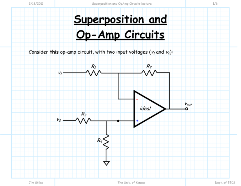
2/18/2011 Superposition and OpAmp Circuits lecture 1/6 Superposition and Op-Amp Circuits Consider this op-amp circuit, with two input voltages (v1 and v2): R2 R1 v1 - v2 ideal R3 vout + R4 Jim Stiles The Univ. of Kansas Dept. of EECS 2/18/2011 Superposition and OpAmp Circuits lecture 2/6 Apply superpostion The easiest way to analyze this circuit is to apply superposition! Recall that opamp circuits are linear, so superposition applies. Our first step is to set all sources to zero, except v2 —in other words, set v1 =0 (connect it to ground potential): R2 R1 - v2 ideal R3 v+ vo2 + i+ = 0 R4 Jim Stiles The Univ. of Kansas Dept. of EECS 2/18/2011 Superposition and OpAmp Circuits lecture 3/6 v1 = 0 Since the current into the non-inverting input of the op-amp is zero (i+ = 0 ), it is evident that: v+ = R4 R3 + R4 Likewise, the remainder of the circuit is simply the non-inverting amplifier, where: vo 2 vo 2 ⎛ R ⎞ ⎛ R4 ⎞ = ⎜1 + 2 ⎟ ⎜ ⎟ v2 + R R R ⎝ 1 ⎠ ⎝ 3 4 ⎠ Jim Stiles R2 R1 - ⎛ R ⎞ = ⎜1 + 2 ⎟ v+ R1 ⎠ ⎝ Combining these two equations, we get: v2 v2 ideal R3 v+ vo2 + R4 The Univ. of Kansas Dept. of EECS 2/18/2011 Superposition and OpAmp Circuits lecture 4/6 v2 = 0 Now for the second step. Turn off all sources except v1 —in other words set v2 =0: R2 R1 v1 i− = 0 v− - ideal R3 v+ vo1 + i+ = 0 R4 Jim Stiles The Univ. of Kansas Dept. of EECS 2/18/2011 Superposition and OpAmp Circuits lecture 5/6 An inverting amp It is evident that the since the current into the non-inverting terminal of the op-amp is zero, the voltage v+ is likewise zero. Thus, the circuit above is simply an inverting amplifier, where: vo 1 = − R1 v1 i− = 0 R2 v R1 1 v− R2 - ideal R3 v+ vo1 + i+ = 0 R4 Jim Stiles The Univ. of Kansas Dept. of EECS 2/18/2011 Superposition and OpAmp Circuits lecture 6/6 And the result There are no more sources in this circuit, so that we can conclude from superposition that the output voltage is the sum of our two, single-source solutions: ⎛ ⎛ R2 ⎞ R ⎞ ⎛ R4 ⎞ vout = vo 1 + vo 2 = ⎜ 1 + 2 ⎟ ⎜ v − ⎟ 2 ⎜ ⎟ v1 + R R R ⎝ ⎝ R1 ⎠ 1 ⎠ ⎝ 3 4 ⎠ v1 Note this circuit is effectively a weighted difference amplifier. R2 R1 - v2 ideal R3 vout + R4 Jim Stiles The Univ. of Kansas Dept. of EECS
