RF MEMS Switching: What You Need to Know
advertisement
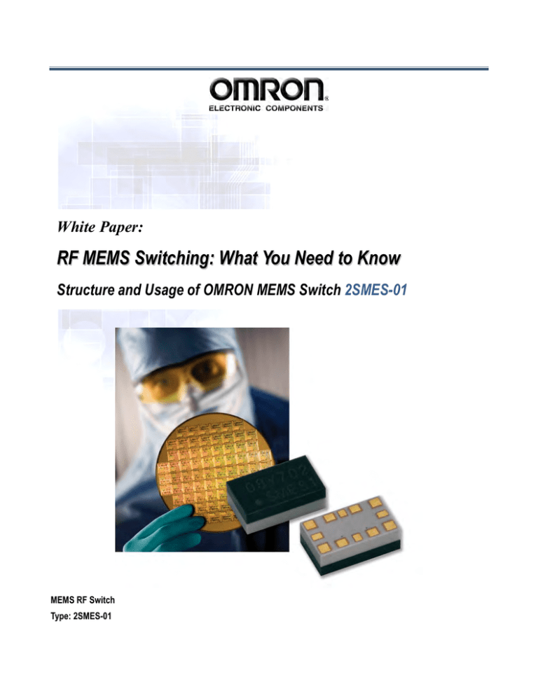
White Paper: RF MEMS Switching: What You Need to Know Structure and Usage of OMRON MEMS Switch 2SMES-01 MEMS RF Switch Type: 2SMES-01 White Paper: 2SMES-01 MEMS RF Switch 1 Outline In this application note, the basic operation principle and driving method for OMRON’s MEMS switch (2SMES-01), that has an electrostatic actuator, will be described. 2 Features • Enable mechanical ON/OFF switching with MEMS technology • Low insertion/return loss and high isolation for GHz signal • Superb endurance (more than 100M switching operations) • Small size (5.2 x 3.0 x 1.8 mm, LGA12) • Low power consumption (less than 10μW) 3 Structure 3.1 Basic Structure of MEMS Switch (SPDT) OMRON’s MEMS switch has a SPDT(Single Pole Double Throw) contact configuration. Two MEMS chips that have a SPST (Single Pole Single Throw) contact configuration are installed on the ceramic package using the flip chip bonding method as shown Fig.1. Fig.1 SPDT Package Structure Copyright © 2013 OMRON Corporation. All Rights Reserved. 2 White Paper: 2SMES-01 MEMS RF Switch 3.2 Basic Structure of MEMS Switch (bare CHIP) The basic structure of MEMS switch consists of three layers which are Glass-Silicon- Glass, as shown Fig. 2. It has a SPST contact configuration, “1a”, normally open type. The top glass part is used for protecting the actuator and hermetic sealing. The middle silicon section contains the actuator and movable electrode. A capacitor is built up between the fixed electrode and movable electrode. The signal line and fixed electrode are made on a glass base. When applying the voltage between Fixed Electrode and Movable Electrode, an electrostatic force is generated and it pulls in the Movable Electrode (actuator). When the driving voltage becomes OFF, the electrostatic force will disappear, and then the actuator will go back to the original position because of a self-restoring force. The signal line and the movable contact consist of pure metal wiring, and serve as a mechanical switch which can handle DC to High Frequency signals. When applying the voltage, electrostatic force “F” is generated, Movable Electrode is pulled to Fixed Electrode. F F Fig.2 Internal Structure of MEMS Switch (CHIP) Copyright © 2013 OMRON Corporation. All Rights Reserved. 3 White Paper: 2SMES-01 MEMS RF Switch 4 Operating Principle 4.1 Operating principle and Structure of Electrostatic Actuator This electrostatic actuator’s basic structure is a parallel plate type capacitor. The electrostatic force generated between the two electrodes is represented by the following equation. Where F is the electrostatic force, ε0 and εr are the dielectric coefficients for a vacuum and a surrounding gas, respectively, and S is the area of the electrode. V is the applied voltage, and d is the average gap between the two electrodes. The MEMS switch can be operated by using this electrostatic force. F= ε 0ε r SV 2 2d 2 S d εr F V Fig. 3 Parallel Plate Type Capacitor 4.2 Internal Equivalent Circuit of MEMS Switch (SPST) The internal equivalent circuit of this switch is the combination of the variable capacitor that is made between the movable electrode and fixed electrode and the internal resistance that the silicon actuator has. Those variable capacitor and internal resistance elements are series-connected. The capacitance value between electrodes changes from several pF to 20pF according to the electrode gap at the time of operation. The internal resistance value of actuator is about 10K ohm. Copyright © 2013 OMRON Corporation. All Rights Reserved. 4 White Paper: 2SMES-01 MEMS RF Switch MEMS Switch (SPST) +V Input Side Variable C (several pF Output Side (Normally Open) Internal R GND (≒10kΩ) Fig. 4 Internal Equivalent Circuit The internal equivalent circuit after packaging is a SPDT structure that has a common terminal on input side and output side. Each GND terminal on input side and one half (RF-COM) of the RF ports on output side are connected, as shown Fig. 5. MEMS Switch RF1 +V1 (Internal R) GND RF-COM (Internal R) RF2 +V2 Fig. 5 Internal Equivalent Circuit (SPDT) Copyright © 2013 OMRON Corporation. All Rights Reserved. 5 White Paper: 2SMES-01 MEMS RF Switch 5 Dimensions (2SMES-01) 6 Specifications Item Description Actuator Ratings Driving System Electrostatic Force Driving (Input Side) Rated Operating Voltage 34VDC±5% Pickup Voltage 90% max. of Rated Voltage Release Voltage 10% min. of Rated Voltage Absolute Maximum Voltage 40V Power Consumption Max. 10μW Signal Side Contact Configuration SPDT (Output Side) Contact Resistance (initial) Typ. 1.0Ω Operating / Release Time Max. 100μs Max. Peak Power Max. Carry Power Copyright © 2013 OMRON Corporation. All Rights Reserved. +36dBm 6 White Paper: 2SMES-01 MEMS RF Switch Rated Load +30dBm DC0.5V0.5mA / Resistive High Frequency Characteristics Impedance Performance Insertion Loss Isolation Return loss -3dB Roll Off Frequency 50Ω Typ. 1.0dB@10GHz Typ. 30dB@10GHz Typ. 10dB@10GHz Min. 12GHz Durability Electrical : DC0.5V0.5mA / Resistive 100,000,000 (cycles) Note. Please confirm most current specifications with the Omron online data sheet. 7 Usage 7.1 Precautions for Driving Circuit Design of MEMS Switch (SPDT) Please note below when designing the driving circuit for MEMS switch. DC34V±5% Fig. 6 Example of Drive Circuit for MEMS Switch (SPDT) (1) This Switch uses an integrated structure for the DC-GND (pin 9) on the input side and the RF-GND (pins: 1, 2,4,5,7, and 11) on the output side. For a relay drive circuit, first be sure to ground the GND pins and then use a high-side switch (Vcont_1 & Vcont_2, not ground) to turn the operating voltage ON and OFF. Copyright © 2013 OMRON Corporation. All Rights Reserved. 7 White Paper: 2SMES-01 MEMS RF Switch (2) This Switch is an electrostatic drive type. To turn OFF the switch, the charge accumulated on the primary side must be discharged. Install a discharge circuit in the switch drive circuit. The resistance value for the discharge circuit must be 1 MΩ or less. If there is no discharge circuit, the switch will not turn OFF. This may result in contact sticking. (3) This Switch is designed so that the electrostatic actuator operates at a high speed. Because of this, the time constant of the drive waveform may affect the operating characteristics and life performance of the Switch. Therefore, the drive circuit must be designed so that the square wave time constant (τ) in the vicinity of the operating input pins (Vcont_1 and Vcont_2) is greater than 0.5 μs and less than 10 μs. (4) The operating voltage must be kept in the range of 34V±5% including ripple. 7.2 Precaution for parallel connection of MEMS Switch As shown in Fig. 7, when connecting N pieces of electrostatic actuators in parallel, set the value of the discharge resistance to 1Mohm/N. When each capacitance of an electrostatic actuator is C, the total capacitance in parallel connection will be "N x C". In this case, if discharge resistance is 1Mohm, the time constant of electric discharge of all the actuators is τ=N x C x1 Mohm, so N times discharge time is needed. The actuation speed of an electrostatic actuator is affected by the electric charge accumulated in the actuator. If the time constant of electric discharge becomes long, actuation speed of an electrostatic actuator becomes slow and contact durability may degrade. Please set the value of discharge resistance so that the time constant of the drive waveform near the input terminal (8pin, 10pin) is between 0.5μs and 10μs. Driver IC Control DC-PS DC34V±5% MEMS (C=20pF, Discharge Resister Switch R=10kΩ)× ・・・ 1MΩ/N Fig. 7 Equivalent Circuit of Parallel Connection of Electrostatic Actuator Copyright © 2013 OMRON Corporation. All Rights Reserved. 8 White Paper: 2SMES-01 MEMS RF Switch 7.3 Circuit Design Example of 34V Power Supply (For Reference) Figure 8 shows the reference circuit design using LT3494/LT3494A DC-DC converter for making a 34V power supply which is needed to drive the MEMS switch. In addition, please refer to the data sheet from Linear Technology’s HP for the detailed specification and the detailed directions for use of LT3494/LT3494A. Fig. 8 Circuit Diagram of Step-up Power Supply using LT3494 Table1. Parts List of Step-up Power Supply using LT3494 Part Name Step-up U1 converter Manufacture Type name Specifications Linear LT3494 DD8 package, 8-lead plastic DFN Technology (LT3494A) Resistor R1/R3 Rohm MCR01 1MΩ, 50V, 1005(0402) Resistor R2 Rohm MCR03 5.1MΩ, 50V, 1608(0603) Capacitor C1 TDK C2012JF1C475Z 4.7uF, 16V, 2125(0805) Capacitor C2 TDK C2012JF1H225Z 2.2uF, 50V, 2125(0805) Capacitor C3 TDK C2012JB1H224Z 0.22uF, 50V, 2125(0805) Inductor L1 TDK GLF1608T200M 22uH, 3Ω, 60mA, 1608(0603) Copyright © 2013 OMRON Corporation. All Rights Reserved. 9 White Paper: 2SMES-01 MEMS RF Switch Selection Guide of Inductor If the following formula is used as a standard in the case of selecting an inductor, the inductor value of the estimate for LT3494 is computable. L = (VOUT – VIN(MIN) + 0.5V) ×0.66 (μH) Where VOUT is the needed output voltage, VIN(MIN) is the minimum input voltage. Please use a standard inductor near the calculated value. Selection Guide of Input/Output Capacitor When the transient response and the stability of this power supply needs to be improved, it is suitable to attach a 4.7μF input capacitor (C1) and a larger output capacitor (C2) from 2.2 μF to 10 μF to the VOUT node. In addition, a capacitor with a sufficient voltage rating should be used. When the power supply circuit using LT3494 is constructed based on the above circuit diagram, as shown in Fig. 9, it generally becomes a mounting space less than a 10mm square. This circuit configuration can output a current of approximately 1mA. NOTE, this is an example of a step up converter design, please be sure to carry out a sufficient initial evaluation for the actual application in use. Approx. 10 mm x 10mm Fig.9 Parts Mounting Image 7.4 Precaution for selection of Driver IC Please take careful design consideration regarding the “Current Capacity” and “Withstand Voltage” when selecting a suitable Driver IC. As described before, when driving MEMS switch, it has an equivalent circuit of a series connection of Capacitance and Resistance. So, if an electrostatic actuator is turned ON, it needs the electric charge of Q expressed as follows. Q=C×V ・・・① Copyright © 2013 OMRON Corporation. All Rights Reserved. 10 White Paper: 2SMES-01 MEMS RF Switch Roughly speaking, since the actual time of inrush current is decided by the time constant “τ” depending on CxR expressed as follows. τ=C×R ・・・② So, inrush current to Driver IC would be about 3.4mA depending on the ratio of input voltage “V” and internal resistance “R”. I = dQ / dt = (CxV) / (CxR) = V / R=34 / 10k = 3.4mA ・・・③ On the other hand, when connecting nth MEMS switches, total inrush current would be 3.4×N (mA) that is proportionate to the parallel connection number of MEMS switch. Ex.) N=64 inrush current = 3.4 x 64 = 217.6mA When selecting a Driver IC, a device with enough current capacity against above inrush current and withstand voltage should be selected. Fig.10 shows the reference circuit design that has a boost converter and several Photo-MOS (ex.G3VM-61PR1) as the Driver IC. Several MEMS switches can be operated by using below configuration. Boost Converter (DC34V) If connecting in parallel Driver IC MEMS Switch Fig .10 Configuration Example of Boost Converter and Driver IC for MEMS switch 8 Glossary Copyright © 2013 OMRON Corporation. All Rights Reserved. 11 White Paper: 2SMES-01 MEMS RF Switch What is MEMS? MEMS is written as “Micro Electro Mechanical Systems”, it is the technology of very small devices that are fabricated by semiconductor device fabrication technologies. Some micro scale mechanical components, sensors, actuators or electrical circuits are integrated on one silicon substrate, glass substrate, organic substrate and so on. Electrostatic Force Driving MEMS Switch An ultra-small mechanical switch that has an electrostatic force driving system fabricated by MEMS technologies. Peak Power The maximum amount of power that a device can handle for an instant without damage. Carry Power The maximum amount of power that a device can handle continuously without damage. Rated Load The load conditions for guaranteeing the contact durability. The load is electrically connected to the signal line and ON/OFF switching can be performed in the active state. Insertion Loss The loss of the electric power spread from one terminal to another in a high frequency circuit which consists of 2 terminal-pair networks after the circuit has been closed. It is usually expressed in decibels (dB). Isolation The loss of the electric power spread from one terminal to another in a high frequency circuit which consists of 2 terminal-pair networks after the circuit has been opened. It is usually expressed in decibels (dB). Return Loss The ratio between the input power and the reflected power at one terminal in the high frequency circuit. It is usually expressed in decibels (dB). Cut-off Frequency The frequency of the point that the insertion loss usually falls by 3 dB rather than the nominal value in the high frequency circuit. Copyright © 2013 OMRON Corporation. All Rights Reserved. 12 White Paper: 2SMES-01 MEMS RF Switch More Information OMRON Electronic Components Web http://www.components.omron.com/ Contact Us For further inquiries such as delivery, price, sample and/or specification, please contact your local Omron authorized distribution partner or Omron sales representative. Americas Sales Office http://www.components.omron.com/components/web/webfiles.nsf/contactus.html Mail Contact components@omron.com Phone Tel: (847) 882-2288 Fax: (847) 882-2192 55 Commerce Drive, Schaumburg, IL 60173 USA * Data and specifications are subjected to change without notice. * Refer online for full Terms & Conditions http://www.components.omron.com/components/web/webfiles.nsf/sales_terms.html Copyright © 2013 OMRON Corporation. All Rights Reserved. 13
