Accurate Delay Computation for Noisy Waveform Shapes
advertisement
Accurate Delay Computation for Noisy Waveform Shapes
Amit Jain, David Blaauw, Vladimir Zolotov*
University of Michigan, Ann Arbor, MI
In this paper we present a new gate delay model for accurate
modeling of difficult waveform shapes, such as those resulting
from coupling capacitance noise, inductive ringing and resistive
shielding. Our modeling approach uses a process of time shifting and time stretching of a set of so-called base-waveforms.
These base-waveforms are selected from a large set of noisy
waveform shapes that occur in interconnect structures with coupling and other types of noise, such that the delay error across
all considered waveforms is minimized. Depending on the
desired accuracy one or more base-waveforms can be used.
This method is also used to model the gate output waveforms
allowing for closure, in terms of the used base-waveforms
across a circuit library. We show that the determination of the
optimal set of base-waveforms under such input-to-output closure is exponential in complexity. We, therefore, propose an
heuristic approach that maps the problem to the unate covering
problem for which efficient solution methods are available. The
new delay model can be applied in a timing analysis program
with minor changes. We present results that demonstrate the
accuracy of the new delay model for waveforms perturbed with
noise for a large set of waveform shapes.
1. Introduction
As clock frequencies continue to increase with process scaling, accurate timing analysis for digital circuits remains a critical concern. A key component in the accuracy of timing
analysis is the accuracy of the gate delay model which models
the highly non-linear behavior of CMOS gates. In traditional
gate delay modeling a gate is simulated in SPICE with a ramp
input waveform for each different input slope and capacitive
output loading [1][2]. For each input slope and output loading
condition the delay and output slope obtained from the SPICE
simulation is then recorded in a two-dimensional delay table.
During timing analysis the waveform at the input of a gate is
first represented with an equivalent ramp waveform that
matches the 20 - 80% Vdd crossing times of the signal. Then,
based on the input slope of the ramp and the output load of the
gate, the delay of the gate and the slope of the output waveform
are obtained from the two-dimensional delay table through linear interpolation.
resistive interconnect loading through the computation of an
effective loading capacitance, referred to as the so-called Ceff
computation [4]. Extensive work in the area of interconnect
delay modeling has also been performed to propagate the ramp
output waveform at the output of one gate to the input of the
next gate through the interconnect structures [5].
While the simple ramp based input and output waveform
approximations were successfully used for many years, new
interconnect effects in nanometer design have increased significantly with technology scaling. As a result, circuit delay is now
affected by a number of noise sources [6][7][8]. Modeling the
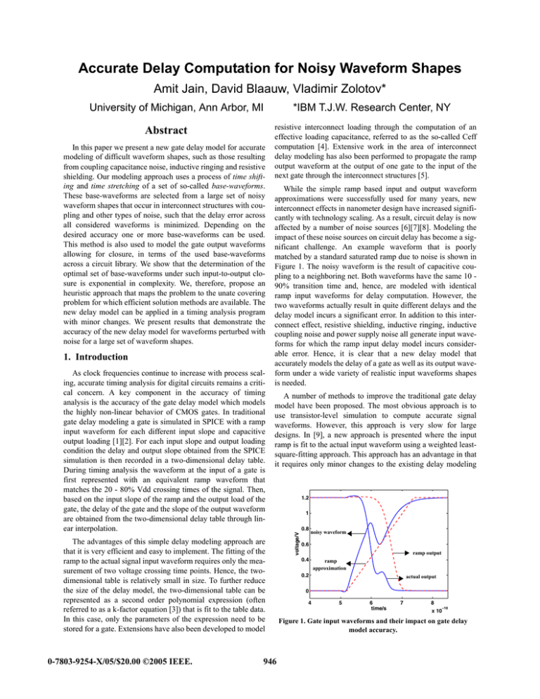
impact of these noise sources on circuit delay has become a significant challenge. An example waveform that is poorly
matched by a standard saturated ramp due to noise is shown in
Figure 1. The noisy waveform is the result of capacitive coupling to a neighboring net. Both waveforms have the same 10 90% transition time and, hence, are modeled with identical
ramp input waveforms for delay computation. However, the
two waveforms actually result in quite different delays and the
delay model incurs a significant error. In addition to this interconnect effect, resistive shielding, inductive ringing, inductive
coupling noise and power supply noise all generate input waveforms for which the ramp input delay model incurs considerable error. Hence, it is clear that a new delay model that
accurately models the delay of a gate as well as its output waveform under a wide variety of realistic input waveforms shapes
is needed.
A number of methods to improve the traditional gate delay
model have been proposed. The most obvious approach is to
use transistor-level simulation to compute accurate signal
waveforms. However, this approach is very slow for large
designs. In [9], a new approach is presented where the input
ramp is fit to the actual input waveform using a weighted leastsquare-fitting approach. This approach has an advantage in that
it requires only minor changes to the existing delay modeling
The advantages of this simple delay modeling approach are
that it is very efficient and easy to implement. The fitting of the
ramp to the actual signal input waveform requires only the measurement of two voltage crossing time points. Hence, the twodimensional table is relatively small in size. To further reduce
the size of the delay model, the two-dimensional table can be
represented as a second order polynomial expression (often
referred to as a k-factor equation [3]) that is fit to the table data.
In this case, only the parameters of the expression need to be
stored for a gate. Extensions have also been developed to model
0-7803-9254-X/05/$20.00 ©2005 IEEE.
946
1.2
1
0.8
voltage/V
Abstract
*IBM T.J.W. Research Center, NY
noisy waveform
0.6
ramp output
0.4
ramp
approximation
0.2
actual output
0
4
5
6
time/s
7
8
−10
x 10
Figure 1. Gate input waveforms and their impact on gate delay
model accuracy.
method as only the fitting of the input ramp is modified. However, while this approach improves the accuracy of the delay
model, it is limited to signal waveforms that do not deviate substantially from a standard ramp-like waveform. Furthermore,
no method for modeling the output waveform shape has been
proposed.
A different approach, presented in [10], uses the shape of a
Weibull cumulative distribution function (CDF) to approximate
arbitrary gate-input waveform shapes. The Weibull CDF is a
function of two parameters and can accurately approximate the
shape of resistively shielded waveforms. However, in the proposed model the gate delay is characterized for two input waveform parameters as well as for the output loading and,
therefore, requires a three-dimensional delay table. This significantly increases the storage requirement and complexity. Also,
the Weibull CDF does not fit well for non-monotone waveform
shapes induced by capacitive coupling noise or inductive ringing. Finally in [11], an approach where waveform shapes are
analyzed using principle component analysis was proposed.
While this approach raises a number of interesting possibilities,
the application in [11] is mainly focused on the modeling of the
output waveform. The application to gate delay modeling was
not discussed.
In this paper, we present a new approach for waveform propagation through CMOS gates which accurately models a large
range of input waveform shapes, such as those resulting from
coupling capacitance, inductive ringing and resistive shielding.
We observe that the traditional process of fitting a ramp is, in
fact, one of stretching and shifting a given ramp waveform in
the time domain. We model this process as a linear transformation of the ramp waveform using time shifting and time stretching and then extend this approach to non-ramp input
waveforms. First, we generate a large number of realistic candidate waveforms WCi that can occur at the input of a gate using
different interconnect structures. We then select from all candidate waveforms a small subset of input base-waveforms WBi
that are used to approximate the complete set of candidate
waveforms using the time shifting and time stretching transformations. Depending on the desired accuracy multiple inputbase-waveforms can be used or a single input base-waveform
may be sufficient.
Similar to the input waveform, the output waveform of a
gate is also approximated using a set of so-called output basewaveforms WBo selected from a set of output candidate waveforms WCo. For a gate a waveform table is maintained for each
input base-waveform. For all stretch factors s of the input basewaveform and for all output loadings this 2-D table stores the
identity of the output base-waveform and its corresponding
time shift and time stretch factors. Note that the time stretch
factor s is analogous to the traditional slew or slope of signals
except that it is applied to a non-ramp signal. The storage
requirement of the waveform table is similar to that of a traditional delay table. Note, also, that across the range of stretch
factors and loading conditions, the output can be approximated
using a number of different output base-waveforms. The
detailed shape of a specific base-waveform is stored only once
in the library and its storage cost is, therefore, amortized over
numerous uses of each base-waveform in the library.
During timing analysis, waveforms are propagated as follows: Given an actual waveform at the input of a gate, the time
shift ta and stretch factor s that best approximate the actual
waveform (using least square error) are computed for all input
base-waveforms in WBi. The base-waveform with the least error
is then selected and, using its 2-D waveform table, the output
base-waveform is identified along with its required time shift
and time stretch factors. The output waveform is then constructed and convolved with the interconnect transfer function,
resulting in a waveform at the input of the next gate.
The primary additional computations required in the proposed approach are the determination of the time shift and
stretch factors for each base-waveform and the selection of the
best base-waveform. While this overhead is minor it can be further reduced by selecting the set of the base-waveforms such
that closure is obtained under propagation of waveforms
through all gates for all possible loads. Consequently, the set of
input and output base-waveforms is the same and the propagation of any waveform wi ∈ W B through a gate transforms
waveform wi into waveform w j ∈ W B from the same set of
base-waveforms. Hence, for short output interconnect that does
not significantly change the shape of the waveform, the best fitting input base-waveform does not need to be explicitly determined - the identity and time stretch factor of the output basewaveform of a gate can be directly used to index the correct
waveform table of a fanout gate. In this case, the proposed
approach will have a runtime efficiency equal to that of the traditional ramp based model and the runtime will be independent
of the number of base-waveforms. For less frequently occurring
long interconnects where the shape of the waveforms can
change significantly, the runtime complexity increases linearly
with the number of base-waveforms used. In all cases, the storage requirement is linear with the number of base-waveforms.
We show that selecting the optimal set of input and output
base-waveforms for any given error tolerance has exponential
complexity with the number of candidate waveforms. Hence,
we propose an heuristic selection approach where the set of
input base-waveforms is selected first and the set of output
base-waveforms is restricted to the former set. Since the output
base-waveforms are typically much easier to match, this
approach was found to yield high quality results. We then show
that the input base-waveform problem can be cast as an unate
covering problem, for which efficient heuristics are available.
We show that even with a single base-waveform, the delay
accuracy is improved by 52% compared with a ramp delay
model. At most, five waveforms were needed to obtain a maximum gate delay error of 34ps for cells from an 0.18µm industrial library. Finally, the approach adapts well to new and
unforeseen waveform shapes. Such new waveform shapes do
not require an entirely new modeling approach. They are
instead seamlessly accommodated in the proposed approach by
simply adding additional base-waveform shapes as needed.
The remainder of the paper is organized as follows. In Section 2, we formulate the problem of selecting an optimal set of
947
base-waveforms. In Section 3, the signal modeling methodology for static timing analysis is presented in detail. In Section 4,
we present our results and in Section 5, we conclude the paper.
2. Problem Formulation
In the traditional gate delay model approach a ramp input
waveform is fit to an actual waveform using two degrees of
freedom. The ramp waveform is first shifted in time to match
the 50% Vdd crossing time of the actual waveform and the
slope of the ramp is then changed to match the delay from the
20 - 80% Vdd crossing time (or 10 - 90% Vdd). Typically, the
result is that the 50% ramp point is different from 50% actual
waveform point. We refer to the two fitting parameters as time
shift ta and time stretch s. It is clear that this same process can
be easily extended to arbitrary base-waveforms.
We specify a waveform as a vector of n time points T =
{t1,t2, t3,..., tn}, where time point ti corresponds to the time that
the waveform crosses i ⋅ Vdd ⁄ n . The time points, therefore,
correspond to the crossing times at constant voltage intervals as
shown in Figure 2. The process of fitting a base-waveform T to
a real waveform is now formulated as follows:
model the large set of actual waveforms that need to be represented for the input and output of a gate. In our approach we
draw this set of base-waveforms from the set of actual waveforms themselves. This is based on the observation that, due to
the low-pass filter characteristics of a gate, the actual waveforms after propagation through a gate resemble each other
closely when accounting for time shifting and timing stretching.
Given a large set of so-called candidate waveforms WC, which
represent the space of possible real waveforms, our task is to
select an optimal set of base-waveforms WB such that the
worst-case error of modeling any candidate waveform by one
of the base-waveforms is minimized. We approach this task
using the following formulation:
Formulation 1:
1. Generate a large, comprehensive set of candidate waveforms
Wc that represent all possible waveform shapes encountered
in a design.
2. For each waveform w i ∈ W c , and for each gate G and each
load capacitance C, compute the propagated waveform
wi,out(G,C) and the error of approximating the input waveform wi by w j ∈ W c and its output waveform wj,out(G,C) by
Given a base-waveform with time point vector T and a fitting
objective, find ta and s such that the waveform R = ta + s ⋅ T
minimizes the fitting objective.
In a traditional gate delay model that uses a ramp input, it is
clear that the time point vector is simply ti = s ⋅ i and the fitting
objective is to match the 50% Vdd crossing time and the 20 80% Vdd transition delay of the actual waveform and of R. It
should be noted that the work in [9] effectively replaces this
simple fitting criteria with a more sophisticated measure using a
weighted least-square error function. This significantly
improves the delay model accuracy. In industrial practice it has
been observed that using more realistic waveforms instead of a
simple ramp improves the accuracy of the waveforms. However, to our knowledge, the selection of such realistic waveforms and their scaling has been performed in an ad hoc
manner.
In this paper, we extend the waveform fitting problem, formulated above, to multiple, arbitrary base-waveforms in a systematic manner. Allowing for multiple base-waveforms raises
the question of which base-waveforms will most effectively
V8
V7
V6
V5
V4
V3
V2
V1
t1
ti
t8
Figure 2. Time as a piece-wise linear function of voltage.
wk ∈ W c , where wj and wk can be arbitrarily shifted and
stretched to minimize the approximation error. The error
between wout(G,C) and wk is computed as the maximum
deviation in voltage crossing time across all voltages from
20 - 80% of Vdd.
3. Find a minimal set of waveforms WB such that any input
waveform wi ∈ W c and its propagated waveform
wi,Prop(G,C) through any gate G and for any load C can be
approximated by waveforms w j, w k ∈ W B with an error margin less than the given value ε.
This formulation can be formulated in the discrete domain
by generating a three-dimensional covering matrix C, such that
Ci,j,k = 0 iff the error of approximating waveform wi and the
result of its propagation wi,Prop with waveforms wj and wk,
respectively, is more than ε, and Ci,j,k = 1 otherwise. We then
need to find the minimal set of indices Nc corresponding to the
selected base-waveforms WB such that for each 1 ≤ i ≤ n there
exists a pair of indices j, k ∈ N c such as Ci,j,k = 1.
It is possible to solve this problem by full enumeration of all
of the possible solutions of WB. However, this approach has
exponential complexity with respect to the size of the WB.
Alternatively, a possible algorithm could be used where we iteratively expand a set of selected indices with the index resulting
in the highest coverage. However, these approaches all need to
process a very large 3D matrix, the generation of which could
be infeasible. We, therefore, propose a different heuristic
approach to solve this problem which involves decomposing
the problem into two simpler problems. This approach is based
on the observation that output waveforms of gates are much
easier to model since they typically represent smoother transitions than do input waveforms that are strongly affected by
948
noise.
1. The first problem is to select a set of waveforms WBi approximating input waveforms so that the propagated waveform of
the original waveform w and its approximation w a ∈ W Bi
result in an error less than the required value ε. (The error ε
is again computed as the maximum deviation in voltage
crossing time across all voltages from 20 - 80% of Vdd for
the actual and approximate waveforms).
2. The second problem involves approximating the output
waveforms Wout resulting from propagation of the selected
waveforms WBi with some of the selected waveforms WBi.
We now show that the first problem can be formulated as an
unate covering problem. We approach this task using the following formulation:
Formulation 2:
1. Generate a large, comprehensive set of candidate waveforms
WC that represent all possible waveform shapes encountered
in a design.
2. Compute a so-called error matrix E, where each entry Ei,,j is
the error of approximating the propagated waveform wj,Prop
by the propagated approximate waveform R = ta + s ⋅ wi,
shifted by time ta and stretched by factor s where ta and s are
obtained using a fitting criterion.
3. Given a maximum allowed delay error ε, generate the covering matrix C, such that Ci,j = 0 iff Ei,,j > ε, and Ci,j = 1 iff
Ei,,j ≤ ε.
4. Find the minimum size set of rows B = {b1, b2,..., bi,...} (corresponding to the selected base-waveforms WB) such that for
each column j (corresponding to the candidate waveforms) at
least one entry Ci,,j = 1.
It is clear that Step 4 corresponds to the unate covering problem
and can be solved using a number of efficient heuristics. In our
approach, the fitting criterion in Step 2 uses a modified leastsquare error objective which was found to be effective. However, any suitable fitting objective function can be used.
It is important to note that the error matrix E is based on the
delay deviation of the propagated base-waveform from the
propagated actual waveform in Step 2. After propagation
through a gate, two very different waveforms can become very
similar due to the low-pass filtering properties of a gate. Therefore, this approach not only increases the accuracy of the computed error, but it also reduces the number of necessary basewaveforms. The error between the actual propagated waveform
and the propagated fitted base-waveform is computed by taking
the maximum error of their voltage crossing times for voltages
between 20 - 80% Vdd. Therefore, this objective not only guarantees a good approximation of the signal delay (the 50% Vdd
crossing time) but also of the waveform shape as a whole.
waveforms can be selected. While this provides the highest
accuracy with the least number of base-waveforms, it complicates the timing analysis to some extent. Therefore, we investigate the number of required base-waveforms to meet the
required error threshold if a single set of base-waveforms is
used for all loading conditions. Using Formulation 2, this can
be accomplished by computing the maximum approximation
error across all loading conditions when each waveform is
selected as a base-waveform in Step 2. Effectively, we perform
a logic AND of the error matrices in Step 3 across all loading
conditions. In a similar manner, a single set of base-waveforms
can be determined for all gates and all loading conditions in a
library. In this case, a single set of base-waveforms is obtained
for the entire library.
The second problem of approximating the output waveforms
can be efficiently solved (in quadratic time) by simply computing the error due to approximating of each propagated waveform by a waveform from WB,i shifted by time ta and stretched
by factor s. We then select the best approximation. Taking into
account that the number of the selected base-waveforms is not
very large, this computation can be done very efficiently.
Therefore, we will not consider here the details of solving this
problem. It is clear that if we selected a good representative set
of base-waveforms WB, the output waveforms could be approximated with good accuracy.
3. Signal Model for Arbitrary Waveform Shapes
In this section, we further detail the steps in Section 2 and
discuss how to perform timing analysis using multiple basewaveforms.
3.1 Generating candidate waveforms
The candidate waveforms must give a comprehensive representation of all possible waveforms that can be accounted for
during actual operation. Note that including more waveforms in
the candidate set only improves the accuracy of the delay model
since it provides a larger set from which to draw the base-waveforms. While increasing the number of the candidate waveforms increases the runtime for the error and cover matrix
generation and the unate covering problem, these steps are only
performed once during the generation of the delay model and
their runtime is amortized over numerous runs of the timing
analysis itself.
In this paper, the candidate waveform set was generated by
varying the parameters of a typical interconnect structure as
The error matrix is a function of the gate response to a candidate waveform and its fitted base-waveform. Hence, the identified set of base-waveforms for a particular error threshold ε will
depend on the gate type, the gate size and the output loading.
Hence, for each gate and output loading a different set of base-
949
A
Figure 3. Interconnect structure to generate candidate waveforms
1
3
2
1
1
0
1
2
0
1
0
3
1
0
1
Figure 6. Example covering matrix, corresponding
to the error matrix in Figure 5
given by the expression in Step 3 in Formulation 2. The covermatrix corresponding to the sample error matrix in Figure 5 is
shown in Figure 6 when an error threshold ε = 4ps is used.
Figure 4. Sample of waveforms generated using the circuit in
Figure 3
shown in Figure 3 and recording the waveforms at node A. The
values of coupling capacitances, ground capacitance, shielding
resistance, relative transition time overlap between the aggressor and victim nets, input slopes and driver strength at the
aggressor nodes were all swept over their possible range of values, thus generating a large pool of diverse waveforms. Some
of the waveforms generated using this setup are shown in Figure 4. Using a wide range of circuit parameters it is possible to
get a comprehensive set of candidate waveforms that provides a
good representation of the set of possible actual waveforms
encountered during timing analysis. Similarly, we have
included inductive noise effects and their impact on the waveform shape in the set of candidate waveforms.
3.2 Creating the error and covering matrices
An entry in error matrix E[i,j] is computed as the maximum
of the deviations of the propagated j-th output waveform from a
shifted and scaled version of the i-th waveform after propagation. It is clear that the entries on the diagonal of E, E[i,i] i<n,
are always zero. For the sake of illustration, a small error matrix
with three candidate waveforms is shown below in Figure 5.
Entry E[1,2] is the maximum number of deviations at the output of the modeled gate when a shifted and scaled version of
Waveform 2 is applied to the input of the gate instead of Waveform 1 for crossing times between 20 and 80% of Vdd.
For a pool of n generated waveforms n(n-1), SPICE simulations combined with n(n-1) shifting and scaling co-efficients
are computed. However, the cost of creating the error matrix is
incurred only once while designing a new standard cell library
or migrating to a new technology. Based on a given maximum
error ε and the error matrix E, a cover-matrix C is computed as
1
1
2
3
2
3
0ps
5ps
4ps
8ps
0ps
7ps
4ps
6ps
0ps
The task of selecting a set of base-waveforms from a pool of
candidate waveforms, given a desired maximum allowed error
ε is equivalent to an unate covering problem [9]. The objective
is to find the minimum set of columns such that for each row
there is at least one column having one at the intersection with
that row. In other words, every waveform in the set of waveforms is a candidate base-waveform and at the same time, the
selected base-waveforms accurately model every candidate
waveform within the desired error if shifted and stretched in
time. It is clear that as the number of waveforms is increased
the approximation error ε decreases.
3.3 Timing analysis using multiple base-waveforms
Using the proposed approach, each gate G is associated with
its own waveform table TProp,G describing how the input waveforms are transformed into output waveforms. The waveform
table specifies the type of output base-waveform, time shift
(gate delay) and time stretch factor (waveform length). Alternatively, the gate delay and scale factor can be expressed using a
k-factor expression which records the delay of the gate for different gate output loadings and time stretch factors s. During
timing analysis we simply propagate base-waveforms through
gates, which is similar to the propagation of ramp signals. During this propagation we compute arrival times by accumulating
gate delays (time shifts) and calculate stretch factors, which is
similar to computing slews in traditional timing analysis. The
only difference with traditional timing analysis is the fact that,
during the propagation, the waveforms can change in type.
However, if we use only one waveform type there is no implementation difference between the proposed method and traditional timing analysis. When propagating signals though
interconnect structures, the signal waveform at the output of the
interconnect is computed by using convolution of the input signal with the transfer function of the interconnect. Delay noise
can be accurately modeled by determining the waveform
change due to noise pulse injection. We then fit the resulting
waveform to one of the base-type waveforms, selecting its type,
time shift and time stretch factor so that the sum of squared
deviations is minimized. The cost of fitting is generally much
less than the cost of signal convolution used for interconnect
simulation.
Figure 5. Sample error matrix for three candidate waveforms
950
Table 2. Results for the input waveform matching for different
gates (10fF output loading).
Table 1. Results for the input waveform matching for inverter
Output
Cap
Ramp Waveform
Proposed Approach
Least
Square
Fit
10 Single
Two
Five
90% fit W-form W-form W-form
10fF
64.4ps
93.3ps
43.3ps
38.0ps
21.0ps
5fF
59.3ps
91.6ps
42.0ps
37.5ps
2fF
64.4ps
90.6ps
44.6ps
Max
across
loading
64.4ps
93.3ps
44.6ps
Ramp Waveforms
Gate
Type
Least
Square Fit
10% to
90% fit
Single
Two
Five
Wform Wform Wform
NAND
59.8ps
85.1ps
41.0ps
33ps
22ps
31.0ps
NOR
57.2ps
79.8ps
37.9ps
31ps
23ps
37.0ps
28.0ps
AND
56.7ps
108.2ps
33.9ps
21ps
7ps
38.0ps
34.0ps
OR
55.9ps
106.6ps
33.0ps
27ps
8ps
Inverter
64.4ps
93.3ps
43.3ps
38ps
21ps
Max.
across
gates
64.4ps
108.2ps
43.3ps
39ps
34ps
4. Results
The proposed gate delay model was implemented and tested
using a set waveforms that exhibit significant coupling noise.
The candidate waveforms were generated using the interconnect circuit shown in Figure 3 as well as a similar inductive circuit. As shown in Figure 4, the waveforms are not necessarily
monotonic and, therefore, present a challenging test for conventional gate delay modeling. The number of candidate waveforms was 381. In addition, we also generated a more extensive
set of 2781 waveforms to test the accuracy of the proposed gate
delay model. Cells from an industrial library in 0.18µm technology were used with output loadings of 2fF, 5fF and 10fF.
In Figure 7 the number of required base-waveforms vs. the
gate delay error ε is shown for an inverter gate when approximating the input waveform of a gate. The maximum gate delay
error is also shown when a single set of base-waveforms is used
for all loading conditions (maximum output). As expected, the
graph shows an increase in the number of required base-waveforms where the maximum allowable error is decreased. In
Table 1, the results of the proposed waveform modeling are
compared with results when using a saturated input ramp. Two
approaches for matching the input ramp are shown. The column
10 - 90% fit uses the traditional method of matching 10 - 90%
slope. The column Least Square Fit uses a least-square fitting
approach similar to that used for fitting the base-waveforms in
the proposed approach. The table shows that even by using one
base-waveform, the error in the gate delay can be reduced from
93ps in the traditional approach to approximately 44ps in the
proposed approach, which is an improvement of 52%. If the
more sophisticated least-square fitting approach is used with
the ramp input, the error reduces from 64ps to 44ps, which is an
improvement of 31%. Note that in the latter case, the two
approaches have the same computational cost for STA and differ only in the used base-waveforms. The error in the proposed
approach using a single set of base-waveforms for all loading
conditions was reduced to 38ps for two base-waveforms.
Hence, even a small number of judiciously chosen base-waveforms can result in significant error improvement. The basewaveforms selected by the proposed approach when four waveforms are used are shown in Figure 8.
Table 2 shows the results for Nand, Nor, And and Or gates
and compares the results with those of the inverter in Table 1.
The results when using a single set of base-waveforms across
all gates is again given in the last row. The error for the proposed approach is approximately the same as that for the
inverter case. However, the traditional ramp-based approach
has a higher error, resulting in an error improvement of 60%
using the proposed approach (from 108ps to 43ps).
In Table 3, we show the results for output waveform model-
50
Maximum Output
45
Output 10fF
40
Output 5fF
Ouptut 2fF
35
Error in ps
Proposed Approach
30
25
20
15
10
5
0
0
2
4
6
8
10
Number of Base Waveforms
Figure 7. Obtained trade-off for inverter between delay model
error and number of base-waveforms for three loading and across
all loadings (maximum output).
951
Figure 8. Waveform shapes selected by the proposed modeling
approach for 4 base-waveforms
using the test waveforms with SPICE was 44.4ps, showing a
good match. Note also that for the vast majority of waveforms,
the error is below 10ps.
Table 3. Error in output waveform modeling using basewaveforms from input waveform modeling to enforce closure.
(10fF loading).
Gate
One
Waveform
Two
Waveform
Five
Waveforms
AND Gate
20.3ps
13.4ps
9.1ps
OR Gate
21.4ps
13.7ps
8.9ps
NOR Gate
21.1ps
14.1ps
9.4ps
NAND Gate
22.3ps
13.9ps
9.2ps
Inverter
25.1ps
15.2ps
9.7ps
Maximum
across gates
25.8ps
15.5ps
10.1ps
5. Conclusion
ing for the five different gate types. To enforce closure, the set
of base-waveforms is taken to be the same as the base-waveforms used in Table 2 for the input waveform modeling. The
table again shows the results when the base-waveforms are
restricted to individual gates as well as when a single set of
base-waveforms is selected for all gates. As expected, the
results show that the error incurred in modeling the output
waveforms is much less than that when modeling the input
waveforms, despite the fact that the base-waveforms for the
output modeling are already predetermined.
In order to verify the correctness of our approach, as many as
2781 new test waveforms were generated using an interconnect
model similar to the one described in Section 3. These waveforms were then applied to the inverter gate and its output
response was recorded using SPICE simulation. The inverter
was also characterized with respect to a base-waveform set
identified previously.
The gate delay obtained using the characterization look-up
table (constructed with the proposed method for modeling both
input and output waveforms) was then compared to those measured using SPICE for all 2781 test waveforms to verify the
correctness of the predicted delay. The error profile comparing
the SPICE results with the delay computed using the characterization tables is as shown in Figure 9. A single base-waveform
was used in this case. Using the proposed approach the error
predicted was 43.3ps while the actual maximum error measure
Figure 9. Delay model error when tested with 2781 test waveform
In this paper, we have presented a new delay model that
accurately models waveform shapes that have traditionally
been difficult to model with a simple ramp approximation, such
as those affected by capacitive coupling, inductive coupling and
resistive shielding. Our approach is based on the generation of
large candidate waveforms from which a small set of so-called
base-waveforms is selected. The selected base-waveforms are
then fit, using time shifting and time stretching, to the actual
waveforms at both the input and output of a gate. We show that
the problem of finding the minimum number of base-waveforms needed to guarantee a particular delay model error
threshold can be mapped to the unate covering problem. We
tested the proposed delay model approach for a large set of
capacitively and inductively coupled signal transitions and have
shown that the delay error can be significantly reduced using
only two or three base-waveform shapes.
Acknowledgements
This research was funded in part by NSF, SRC, and Intel.
References
[1] H. Haitian, et.al., “Table Look-up Based Compact Modeling for On-Chip Interconnect Timing and Noise Analysis,”
ISCAS 2003.
[2] www.synopsys.com
[3] C. Ratzlaff, S.Pullela, and L. Pillegi, “Modeling the RCinterconnect effects in a hierarchical timing analysis,”
Proc. IEEE Custom Integrated Circuits Conf., May 1992.
[4] F. Dartu, N. Menezes, and L. Pillegi, “Performance Computation of Precharacterized CMOS gates for RC Loads”,
IEEE Trans on CAD, Vol.15, No. 5, May 1996.
[5] A. Odabasioglu, M. Celik, L. Pileggi, “PRIMA: Passive
Reduced-Order Interconnect Macromodeling Algorithm”,
IEEE Transactions on CAD, 1998.
[6] K.L. Shepard, V. Narayanan, “Noise in Deep Submicron
Digital Design”, Proc. of ICCAD 1996, pp. 524 -53.
[7] G. Bai, S Bobba, I. Hajj, “Static timing analysis including
power supply noise effect on propagation delay in VLSI
circuits,” DAC 2001.
[8] L. He, N. Chang, S. Lin, O. Nakagawa, “An efficient
inductance modeling for on-chip interconnects,” in Proc.
IEEE Custom Integrated Circuits Conference, 1999.
[9] M. Hashimoto, Y. Yamada, H. Onodera, “Equivalent
Waveform Propagation For Static Timing Analysis”,
ICCAD 2003.
[10] C. Amin, F. Dartu, Y. Ismail, “Weibull Based Analytical
Waveform Model”, ICCAD 2003.
[11] S. Nassif, E. Acar, “Advanced Waveform Models for the
Nanometer Regime”, TAU 2004.
[12] G. Hachtel and F. Somenzi, “Logic Synthesis and Verification Algorithms”, Kluwer Academic Publishers
952
