High-Performance RF Modulator Enables Multi-Carrier
advertisement

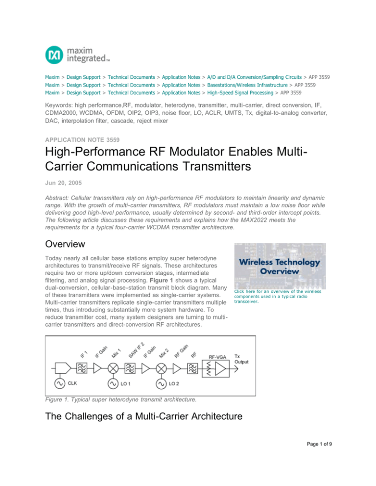
Maxim > Design Support > Technical Documents > Application Notes > A/D and D/A Conversion/Sampling Circuits > APP 3559 Maxim > Design Support > Technical Documents > Application Notes > Basestations/Wireless Infrastructure > APP 3559 Maxim > Design Support > Technical Documents > Application Notes > High-Speed Signal Processing > APP 3559 Keywords: high performance,RF, modulator, heterodyne, transmitter, multi-carrier, direct conversion, IF, CDMA2000, WCDMA, OFDM, OIP2, OIP3, noise floor, LO, ACLR, UMTS, Tx, digital-to-analog converter, DAC, interpolation filter, cascade, reject mixer APPLICATION NOTE 3559 High-Performance RF Modulator Enables MultiCarrier Communications Transmitters Jun 20, 2005 Abstract: Cellular transmitters rely on high-performance RF modulators to maintain linearity and dynamic range. With the growth of multi-carrier transmitters, RF modulators must maintain a low noise floor while delivering good high-level performance, usually determined by second- and third-order intercept points. The following article discusses these requirements and explains how the MAX2022 meets the requirements for a typical four-carrier WCDMA transmitter architecture. Overview Today nearly all cellular base stations employ super heterodyne architectures to transmit/receive RF signals. These architectures require two or more up/down conversion stages, intermediate filtering, and analog signal processing. Figure 1 shows a typical dual-conversion, cellular-base-station transmit block diagram. Many of these transmitters were implemented as single-carrier systems. Multi-carrier transmitters replicate single-carrier transmitters multiple times, thus introducing substantially more system hardware. To reduce transmitter cost, many system designers are turning to multicarrier transmitters and direct-conversion RF architectures. Click here for an overview of the wireless components used in a typical radio transceiver. Figure 1. Typical super heterodyne transmit architecture. The Challenges of a Multi-Carrier Architecture Page 1 of 9 Multi-carrier architectures reduce the number of transmit channels. Direct-conversion architectures reduce the number of components in each channel by converting RF signals directly up from baseband. Both architectures require components with wider dynamic range and higher linearity to meet overall system requirements. Figure 2 shows a typical block diagram of a direct-conversion transmitter architecture. Note the significant reduction in stages in this direct-conversion architecture. Multiple mixers, amplifiers, IF and RF filters are all replaced by a single integrated solution. Figure 2. Direct-conversion architecture. Until recently, digital-to-analog converter (DAC) and the direct-conversion modulator performance was not adequate to support the demanding requirements of 3G multi-carrier, cellular base stations. Today's generation of communications base-station transmitter designs requires both lower cost and more flexible solutions. Selecting the RF modulator significantly impacts cost and flexibility, thereby establishing the transmitter's basic architecture. Solving the Problem with a Single-Transmitter Architecture Maxim Integrated Products introduced a direct quadrature RF modulator, the MAX2022, to address these multi-carrier transmitter needs. The device offers exceptional dynamic range, giving the transmitter designer great control over system performance. The combination of very high OIP2 and OIP3, along with the exceptional output noise floor approaching 174dBm/Hz enables true multi-carrier performance with substantial margins to all relevant system specs. A single-transmitter architecture can now support multiple types of modulations, from CDMA2000 to WCDMA to OFDM, with up to nine carriers. The very high performance of this modulator can, moreover, be exploited in the transmitter design to significantly reduce hardware requirements and costs, and to greatly increase the flexibility of the lineup. The MAX2022 quadrature modulator utilizes a SiGe process to cover a frequency range of 1500MHz to 2500MHz. Figure 3 illustrates the internal architecture of the circuit. Page 2 of 9 Figure 3. MAX2022 block diagram. The MAX2022 features a single-ended LO input, 50Ω internally matched, accepting an input LO drive of 3dBm to +3dBm. The LO is split by a quadrature splitter, and applied to two very high-performance passive mixers. The device's quadrature I and Q inputs are differential inputs, with a 44Ω input impedance. The exceptional input bandwidth of >1GHz allows the device to be used as either a baseband direct-RF modulator or as an image-reject mixer with quadrature IF inputs. The quadrature inputs were designed specifically to interface directly with current-output DACs. This feature eliminates the requirement for intermediary buffer amplifiers, which can both limit performance and increase costs. The mixer outputs are combined and applied to a single-ended RF output, which is internally matched to 50Ω. MAX2022 RF Modulator Performance The performance of an RF modulator is determined by several independent parameters. The MAX2022 excels in all critical areas. The OIP3 is +22dBm, with a P1dB of +12dBm. Intermodulation products between multiple carriers depend on the OIP3; a high OIP3 value ensures low levels of intermodulation distortion. The OIP2 is another critical parameter for zero-IF applications. The MAX2022's OIP2 is +50dBm in the UMTS band. The OIP2 is also significant for baseband signals. Second harmonic effects in the baseband signals will produce spectral spreading in the RF output, thus compromising the ACLR performance. Consequently, high OIP2 values ensure low levels of ACLR distortion. Figure 4 illustrates the performance variation of the device for OIP2, OIP3, and output power over the frequency range of 1500MHZ to 2500MHz. Page 3 of 9 Figure 4. OIP2, OIP3, POUT vs. frequency with the MAX2022. The noise floor performance of the MAX2022 is significantly enhanced by use of passive mixers for the modulation function. These devices generate no excess noise, allowing the device to approach an output noise level of -174dBm/Hz for typical output signal levels. For signal levels above -10dBm, the phase noise of the LO buffers becomes important. These buffers were designed to have exceptionally low phase noise of -164dBc/Hz. Figure 5. Noise floor vs. output power. One measurement useful in comparing RF modulator performance is the device's dynamic range, which is the difference between the maximum practical signal level, as expressed by P1dB, and the noise floor. The MAX2022 has a dynamic range of 186dB, significantly exceeding that of any other integrated RF modulator. LO leakage levels are <-40dBm in the PCS and UMTS bands, and sideband suppression is >45dB for Page 4 of 9 these bands. A digital predistortion control loop can further reduce these levels, driving the LO leakage to below -80dBm and sideband suppression to >60dB. The RF passband flatness is >0.5dB over 100MHz, allowing the use of the part in broadband systems. Multi-Carrier WCDMA Generation in the UMTS Band The ultimate benefit of these many performance parameters is their mutual interaction when generating real-world carriers. Here is where the MAX2022 truly excels. As an illustration, let us consider the problem of generating four carriers with WCDMA modulation. Contemporary transmitter designs must accommodate the bandwidth of the WCDMA carriers themselves, equal to 20MHz. In addition, the system must support the bandwidth necessary to digitally predistort the transmit signal to correct for subsequent distortion by the power amplifier. This bandwidth can exceed 100MHz. Figure 6 illustrates the spectrum of such a signal. Figure 6. 4-carrier UMTS spectrum. We can see that the unusually wide bandwidth pushes the transmit output spectrum beyond the UMTS band limits. This, therefore, requires that the noise performance of the transmitter system conform to the transmitter mask requirements, beyond the band edges, without employing RF filters to trim spurious signals and noise levels. This requirement places exceptional demands on the RF modulator. The wide bandwidth and extra dynamic range of the MAX2022, however, enable such system design. Figure 7 illustrates the ACLR performance for 1-, 2-, and 4-carrier WCDMA generation in the UMTS band. The exceptionally good ACLR values are maintained over a very wide-output power level range due to the wide dynamic range of the MAX2022. This broad range of usable output power is useful in the design of the system. The noise-floor performance is shown to illustrate the total available dynamic range for a chosen ACLR performance. A 4-carrier WCDMA signal at -28dBm per carrier, for example, will have an ACLR of 66dB and an output noise floor of -173.5dBm/Hz. Page 5 of 9 Figure 7. 1-, 2-, and 4-Carrier WCDMA ACLR and noise floor. This exceptionally high level of performance is equally well-suited to generating other modulations, such as OFDM, QAM, etc. CDMA2000 and TD-SCDMA can be supported to over nine carriers. It is one hardware configuration that generates any, or all, of these modulations. System-Level Design The interfaces of the MAX2022 have been designed to minimize the ancillary circuitry requirements. This design significantly reduces overall system costs. The impedance-matched, integrated LO buffers and balun enable the use of a single-ended LO interface at low LO power levels of -3dBm to +3dBm. The integrated RF balun allows a single-ended RF output, which is impedance-matched to 50Ω. The baseband I and Q inputs present a differential interface with a 44Ω internal impedance. These inputs accept a direct connection to the outputs of high-performance current-output DACs with no intervening buffer amplifiers. At the very high-performance levels of the MAX2022, it is quite difficult to find external baseband amplifiers which do not significantly degrade device performance. Fortunately, baseband amplifiers are not necessary in this design. Figure 8 illustrates a recommended DAC termination interface to the MAX2022. The 50Ω resistors to ground terminate the DAC appropriately, and the typical full-scale current of 20mAP-P will deliver up to 0dBm to the baseband input of the MAX2022. Page 6 of 9 Figure 8. DAC interface to baseband inputs. To realize the performance potential inherent in the MAX2022, careful system-level design must be employed. Figure 9 illustrates a suggested lineup for generation of four carriers of WCDMA modulation with digital predistortion capability. The signal levels, noise levels, and ACLR are indicted for the cascaded lineup at each stage's output. Figure 9. Tx lineup with signal analysis. Starting with the DAC, we require a part that can generate a signal with 50MHz of bandwidth, ACLR significantly better than the target 65dB for this design, and noise and spurious floors, which are low. The MAX5895 dual interpolating DAC is suggested as an example part that fulfills these requirements. To allow the DAC to operate at a high-output sample rate and a relatively low-input data rate, interpolating DACs are recommended for this application. The attenuation of the interpolation filters then becomes significant, because the lowpass filter following the DAC will not have significant attenuation of the near-in interpolation images. Interpolating DACs will generate images of the baseband signals at each multiple of the baseband input data rate. If not adequately removed from the modulator input, these images will Page 7 of 9 produce significant sidebands in the RF output of the modulator. The 95dB attenuation of interpolation images by the MAX5895 is ideal for this purpose. This radically reduces the complexity of the baseband lowpass filters following the DACs, thus simplifying DAC design and minimizing their effect on the phase response of the overall system for wideband signals. Moving on to the modulator output, we can see that the output signal level will be -28dBm per carrier, 22dBm total. The ACLR will be set by the modulator's performance at +66dB. (The DAC's performance is not a limitation here.) The noise floor, however, has degraded from the -174dBm/Hz of the modulator alone to -170dBm. This is due to the cascaded noise level of the DAC. Here it becomes apparent that one must choose all elements of the configuration carefully to achieve the overall highest level of performance. The RF amplifier selected must have a low noise figure and adequate OIP3 to avoid degradation of the cascaded ACLR. An OIP3 greater than +30dBm is recommended for this stage, if the gain is 12dB. The output stage with a high OIP3 is chosen to avoid degrading the cascaded ACLR. The MAX2057 RF VGA is suggested to allow the adjustment of the overall lineup's gain to set the output level at -6dBm per carrier, or 0dBm total. The OIP3 of +37dBm ensures that the cascaded ACLR remains at +65dB. This cascaded transmitter design yields an excellent ACLR of +65dB while maintaining a noise floor of 139dBc/Hz relative to each individual carrier. The noise floor and spurious level performance are achieved with no RF filtering required. This allows the same hardware implementation to be used in multiple bands without change. Further, the simplicity of this design with few devices makes it a very compact and costeffective solution for a high-performance transmitter. Conclusion This new modulator, the MAX2022, achieves an unparalleled level of performance in transmitter applications. It allows both Zero IF and image-reject mixer architectures. The device facilitates a highly streamlined, cost-effective, and flexible transmitter architecture, thus increasing design efficiency for the transmitter designer. A similar version of this article appeared in the April, 2005 edition of Microwaves & RF magazine. Related Parts MAX2022 High-Dynamic-Range, Direct Upconversion 1500MHz to 2500MHz Quadrature Modulator Free Samples MAX2057 1300MHz to 2700MHz Variable-Gain Amplifier with Analog Gain Control Free Samples MAX5895 16-Bit, 500Msps Interpolating and Modulating Dual DAC with CMOS Inputs Free Samples More Information For Technical Support: http://www.maximintegrated.com/support For Samples: http://www.maximintegrated.com/samples Other Questions and Comments: http://www.maximintegrated.com/contact Application Note 3559: http://www.maximintegrated.com/an3559 APPLICATION NOTE 3559, AN3559, AN 3559, APP3559, Appnote3559, Appnote 3559 Page 8 of 9 Copyright © by Maxim Integrated Products Additional Legal Notices: http://www.maximintegrated.com/legal Page 9 of 9


