iC-HK, iC-HKB 155MHz LASER SWITCH - iC-Haus
advertisement
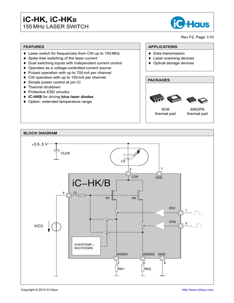
iC-HK, iC-HKB 155 MHz LASER SWITCH Rev F2, Page 1/10 FEATURES • • • • • • • • • • • APPLICATIONS Laser switch for frequencies from CW up to 155 MHz Spike-free switching of the laser current Dual switching inputs with independent current control Operates as a voltage-controlled current source Pulsed operation with up to 700 mA per channel CW operation with up to 150 mA per channel Simple power control at pin CI Thermal shutdown Protective ESD circuitry iC-HKB for driving blue laser diodes Option: extended temperature range • Data transmission • Laser scanning devices • Optical storage devices PACKAGES SO8 thermal pad MSOP8 thermal pad BLOCK DIAGRAM +3.5..5 V CLDA LD 7 3 LDK iC−HK/B 8 VDD CI M1 M2 EN1 EN2 V(CI) 1 5 OVERTEMP.− SHUTDOWN AGND1 AGND2 GND 2 4 RK1 Copyright © 2015 iC-Haus 6 RK2 http://www.ichaus.com iC-HK, iC-HKB 155 MHz LASER SWITCH Rev F2, Page 2/10 DESCRIPTION Laser Switch iC-HK/B enables the spike-free switching of laser diodes with well-defined current pulses at frequencies ranging from DC to 155 MHz. The diode current is determined by the voltage at pin CI and by the resistors RK1 and RK2. The two fast switches are controlled independently via CMOS inputs EN1 and EN2. The laser diode can thus be turned on and off or switched between different current levels defined by the ratio of RK1 and RK2. Each channel can be operated at 150 mA DC and up to 700 mA pulsed current depending on the frequency, duty cycle and heat dissipation. The integrated thermal shutdown feature prevents damage from excessive temperature. PACKAGING INFORMATION SO8-TP, MSOP8-TP to JEDEC PIN CONFIGURATION SO8-TP 8 7 PIN FUNCTIONS No. Name Function 6 5 <P-CODE> <P-CODE> <A-CODE> 1 2 3 4 5 6 7 8 EN1 AGND1 LDK AGND2 EN2 GND VDD CI Channel 1 Switching Input Channel 1 Reference Ground Driver Output (LD Cathode) Channel 2 Reference Ground Channel 2 Switching Input Ground +5 V Supply Voltage Voltage Reference for Current Control The Thermal Pad is to be connected to a Ground Plane on the PCB. 1 2 3 4 PIN CONFIGURATION MSOP8-TP 8 7 6 5 <P-CODE> <A-CODE> 1 2 3 4 iC-HK, iC-HKB 155 MHz LASER SWITCH Rev F2, Page 3/10 PACKAGE DIMENSIONS SO8-TP FRONT 4° 0.08 1.40 45° SIDE 0.84 RECOMMENDED PCB-FOOTPRINT TOP 2.40 4.90 1.27 0.60 All dimensions given in mm. Tolerances of form and position according to JEDEC MS-012 5.40 2.40 6 0.40 1.90 1.27 3.90 2.29 2.29 dra_so8-tp-3_pack_1, 10:1 iC-HK, iC-HKB 155 MHz LASER SWITCH Rev F2, Page 4/10 PACKAGE DIMENSIONS MSOP8-TP FRONT 0.08 4° 0.85 SIDE 0.60 TOP RECOMMENDED PCB-FOOTPRINT 1.75 4.90 0.65 1.60 0.30 3 1.73 0.65 4 2.40 3 2.39 0.40 All dimensions given in mm. Tolerances of form and position according to JEDEC MO-187. dra_msop8-tp-1_pack_1, 10:1 iC-HK, iC-HKB 155 MHz LASER SWITCH Rev F2, Page 5/10 ABSOLUTE MAXIMUM RATINGS Beyond these values damage may occur; device operation is not guaranteed. Item No. Symbol Parameter Conditions Unit Min. Max. G001 VDD Voltage at VDD -0.7 6 V G002 I(VDD) Current in VDD -10 150 mA G003 V(CI) Voltage at CI -0.7 6 V G004 I(LDK) Current in LDK DC current -10 300 mA G005 I(AGND1) Current in AGND1 DC current -150 10 mA G006 I(AGND2) Current in AGND2 DC current -150 10 mA G007 V() Voltage at EN1, EN2, AGND1 and AGND2 -0.7 6 V G008 V(LDK) Voltage at LDK iC-HK iC-HKB -0.7 -0.7 6 15 V V G009 Vd() Susceptibility to ESD at all pins HBM, 100 pF discharged through 1.5 kΩ 1 kV G010 Tj Operating Junction Temperature -40 150 °C G011 Ts Storage Temperature Range -40 150 °C THERMAL DATA Operating Conditions: VDD = 3.5...5.5 V Item No. Symbol Parameter Conditions T01 Ta Operating Ambient Temperature Range (extended range on request) T02 Rthja Thermal Resistance Chip/Ambient (SO8) soldered to PCB, no additional cooling areas therm. pad soldered to approx. 2 cm² cooling area Thermal Resistance Chip/Ambient (MSOP8) soldered to PCB, therm. pad soldered to approx. 2 cm² cooling area T03 Unit Min. Rthja Typ. -25 All voltages are referenced to ground unless otherwise stated. All currents flowing into the device pins are positive; all currents flowing out of the device pins are negative. Max. 85 °C 30 170 50 K/W K/W 30 60 K/W iC-HK, iC-HKB 155 MHz LASER SWITCH Rev F2, Page 6/10 ELECTRICAL CHARACTERISTICS Operating Conditions: VDD = 3.5...5.5 V, Tj = -25...125 °C unless otherwise stated Item No. Symbol Parameter Conditions Tj °C Fig. Unit Min. Typ. Max. Total Device 001 VDD Permissible Supply Voltage 3.5 5.5 V 002 I(VDD) Supply Current in VDD CW operation 0 80 µA 003 I(VDD) Supply Current in VDD pulsed operation, f(EN1, EN2) = 150 MHz 0 150 mA 004 V(LDK) Permissible Voltage at LDK iC-HK iC-HKB 0 0 5.5 12 V V 005 Vc(CI)hi Clamp Voltage hi at CI Vc(CI) = V(CI) – VDD, I(CI) = 10 mA, other pins open 0.4 1.25 V 006 Vc(EN)hi Clamp Voltage hi at EN1, EN2 Vc(EN) = V(EN) – VDD, I(EN) = 1 mA, other pins open 0.4 1.25 V 007 Vc()lo Clamp Voltage lo at VDD, LDK, CI, EN1, EN2, AGND1, AGND2 I() = -10 mA, other pins open -1.25 -0.4 V 008 Ipd() Pull-Down Current at CI, EN1, EN2 1 5 µA 009 Toff Overtemperature Shutdown 110 150 °C 150 mA Laser Control LDK, CI, EN1, EN2 101 Icw(LDK) Permissible CW Current in LDK (per channel) 102 Ipk(LDK) Permissible Pulsed Current in LDK (per channel) f > 100 kHz, thi/T < 1:10 700 mA 107 Vs(LDK) Saturation Voltage at LDK I(LDK) = 40 mA I(LDK) = 60 mA I(LDK) = 150 mA, iC-HK I(LDK) = 150 mA, iC-HKB 1.2 1.3 1.5 1.8 V V V V 108 I0(LDK) Leakage Current in LDK ENx = lo, V(LDK) = VDD 10 µA 109 tr() LDK Current Rise Time Iop = 150 mA, I(LDK): 10% → 90%Iop 3 1.5∗ ns 110 tf() LDK Current Fall Time Iop(LDK) = 150 mA, I(LDK): 90% → 10%Iop 3 1.5∗ ns 111 tp() Propagation Delay V(ENx) → I(LDK) ENx hi ↔ lo, V(50%) → I(50%) 3∗ ns 112 Vt(ENx) Input Threshold Voltage 33 67 %VDD 113 V(CI) Permissible Voltage at CI 0 5.5 V 114 Vt(CI) Threshold Voltage at CI I(LDK) < 5 mA 0.75 1.15 V 115 CR() Current Matching Channel1/Channel2 V(CI) = 0...VDD, I(LDK) = 30...300 mA, RK1 = RK2 0.9 ∗ Projected values by sample characterization 0 1∗ 50 1 1.1 iC-HK, iC-HKB 155 MHz LASER SWITCH Rev F2, Page 7/10 ELECTRICAL CHARACTERISTICS DIAGRAMS I(LDK) 300 mA RKx= 0 Ω 250 I(LDK) tr RKx= 1 Ω 200 tf RKx= 2 Ω I op 150 RKx= 3 Ω 100 RKx= 4 Ω RKx= 5 Ω RKx= 6 Ω 90 % I op RKx= 8 Ω RKx= 10 Ω RKx= 15 RKx= 20 RKx= 30 RKx= 50 50 0 10 % I op 1 1.2 1.4 1.6 1.8 2 2.2 2.4 2.6 V V(CI) t Figure 1: Laser current pulse in LDK Figure 2: Diode current vs. V(Cl) at Tj = 27 °C I(LDK) 700 mA Ω Ω Ω Ω RKx = 0Ω I(LDK) 1200 mA RKx = 0Ω 600 1000 500 RKx = 1Ω 800 400 RKx = 1Ω RKx = 2Ω 300 RKx = 3Ω 200 RKx = 4Ω RKx = 5Ω RKx = 6Ω RKx = 8Ω RKx = 10 Ω 100 0 2.2 RKx = 15 Ω RKx = 20 Ω RKx = 30 Ω RKx = 50 Ω 2.4 2.6 2.8 3 3.2 3.4 3.6 600 RKx = 3Ω 400 RKx = 4Ω RKx = 5Ω RKx = 6Ω RKx = 8Ω RKx = 10 Ω RKx = 15 Ω RKx = 20 Ω RKx = 30 Ω RKx = 50 Ω 200 0 3.5 3.8V V(CI) Figure 3: Diode current vs. V(Cl) at Tj = 27 °C RKx = 2Ω 4 5V 4.5 V(CI) Figure 4: Diode current vs. V(Cl) at Tj = 27 °C I(LDK) 1.5 A I(LDK) 250 mA 200 1 RKx = 0Ω RKx = 0Ω max max 150 min 0.5 100 min 50 0 0 0 0.5 1 1.5 2 0 V(CI) Figure 5: Diode current variation vs. V(CI) at V(LDK) = 3 V 1 2 3 4 5V V(CI) Figure 6: Diode current variation vs. V(CI) at V(LDK) = 3 V iC-HK, iC-HKB 155 MHz LASER SWITCH Rev F2, Page 8/10 V(CI) 0V 0.8 1V 2V 3V I(LDK) [A] 0.6 4V 5V 0.4 0.2 0 1 2 3 4 5 6 V(LDK) [V] Figure 7: Output Characteristics of LDK DESCRIPTION OF FUNCTIONS Laser current dependency of V(Cl), RK1, RK2 Depending on the laser diode different diode currents are necessary to obtain the required laser power. The values for V(CI), RK1 and RK2 can be determined for the required diode current at room temperature from the opposite diagram. A parallel to the x axis must be drawn through the desired diode current. Either RKx can be obtained for a required value of V(CI) or the respective value of V(VI) can be achieved for a given RKx. I(LDK) 300 mA RKx= 0 Ω 2 250 RKx= 1 Ω 200 RKx= 2 Ω 150 RKx= 3 Ω 100 RKx= 4 Ω RKx= 5 Ω RKx= 6 Ω 1 RKx= 8 Ω RKx= 10 Ω RKx= 15 RKx= 20 RKx= 30 RKx= 50 50 0 1 1.2 1.4 1.6 3 1.8 1.75 Thermal Shutdown iC-HK/B is protected by an integrated thermal shutdown feature. When the shutdown temperature is reached both channels are unconditionally switched off. 2 2.2 2.4 2.6 V V(CI) Figure 8: Diode current vs. V(Cl) at Tj = 27 °C APPLICATION NOTES Application notes for iC-HK/B are available as a separate document. Ω Ω Ω Ω iC-HK, iC-HKB 155 MHz LASER SWITCH Rev F2, Page 9/10 REVISION HISTORY Rel Rel.Date Chapter Modification Page F2 15-04-22 FEATURES Combination with iC-WK/L removed 1 F2 PACKAGES Drawings exchanged for more recent ones 1 F2 BLOCK DIAGRAM Combination with iC-WK/L removed 1 F2 DESCRIPTION Obsolete schematics removed 2 F2 PACKAGING INFORMATION Drawings exchanged for more recent ones 2 PACKAGING INFORMATION Package Dimensions added 3, 4 F2 ELECTRICAL CHARACTERISTICS 109, 110, 111: Footnotes regarding test coverage added 6 F2 ELECTRICAL CHARACTERISTICS Output characteristics added 8 F2 ORDERING INFORMATION Updated order designations 10 iC-Haus expressly reserves the right to change its products and/or specifications. An info letter gives details as to any amendments and additions made to the relevant current specifications on our internet website www.ichaus.com/infoletter; this letter is generated automatically and shall be sent to registered users by email. Copying – even as an excerpt – is only permitted with iC-Haus’ approval in writing and precise reference to source. iC-Haus does not warrant the accuracy, completeness or timeliness of the specification and does not assume liability for any errors or omissions in these materials. The data specified is intended solely for the purpose of product description. No representations or warranties, either express or implied, of merchantability, fitness for a particular purpose or of any other nature are made hereunder with respect to information/specification or the products to which information refers and no guarantee with respect to compliance to the intended use is given. In particular, this also applies to the stated possible applications or areas of applications of the product. iC-Haus products are not designed for and must not be used in connection with any applications where the failure of such products would reasonably be expected to result in significant personal injury or death (Safety-Critical Applications) without iC-Haus’ specific written consent. Safety-Critical Applications include, without limitation, life support devices and systems. iC-Haus products are not designed nor intended for use in military or aerospace applications or environments or in automotive applications unless specifically designated for such use by iC-Haus. iC-Haus conveys no patent, copyright, mask work right or other trade mark right to this product. iC-Haus assumes no liability for any patent and/or other trade mark rights of a third party resulting from processing or handling of the product and/or any other use of the product. iC-HK, iC-HKB 155 MHz LASER SWITCH Rev F2, Page 10/10 ORDERING INFORMATION Type Package Options Order Designation iC-HK iC-HK SO8 MSOP8 Thermal Pad Thermal Pad iC-HK SO8-TP iC-HK MSOP8-TP iC-HKB iC-HKB SO8 MSOP8 Thermal Pad Thermal Pad iC-HKB SO8-TP iC-HKB MSOP8-TP For technical support, information about prices and terms of delivery please contact: iC-Haus GmbH Am Kuemmerling 18 D-55294 Bodenheim GERMANY Tel.: +49 (0) 61 35 - 92 92 - 0 Fax: +49 (0) 61 35 - 92 92 - 192 Web: http://www.ichaus.com E-Mail: sales@ichaus.com Appointed local distributors: http://www.ichaus.com/sales_partners
