DirectFET Technology: A Mechanically robust Surface Mount
advertisement
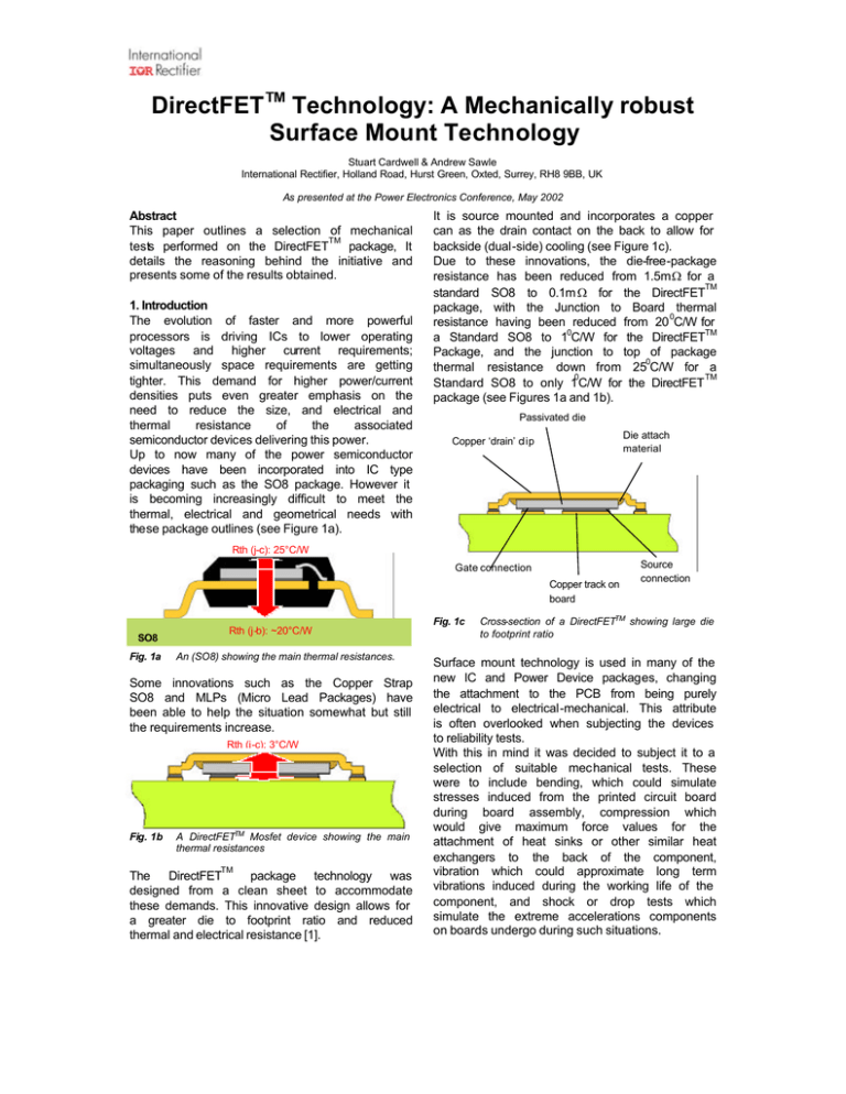
DirectFET TM Technology: A Mechanically robust Surface Mount Technology Stuart Cardwell & Andrew Sawle International Rectifier, Holland Road, Hurst Green, Oxted, Surrey, RH8 9BB, UK As presented at the Power Electronics Conference, May 2002 Abstract This paper outlines a selection of mechanical TM tests performed on the DirectFET package, It details the reasoning behind the initiative and presents some of the results obtained. 1. Introduction The evolution of faster and more powerful processors is driving ICs to lower operating voltages and higher current requirements; simultaneously space requirements are getting tighter. This demand for higher power/current densities puts even greater emphasis on the need to reduce the size, and electrical and thermal resistance of the associated semiconductor devices delivering this power. Up to now many of the power semiconductor devices have been incorporated into IC type packaging such as the SO8 package. However it is becoming increasingly difficult to meet the thermal, electrical and geometrical needs with these package outlines (see Figure 1a). It is source mounted and incorporates a copper can as the drain contact on the back to allow for backside (dual-side) cooling (see Figure 1c). Due to these innovations, the die-free-package resistance has been reduced from 1.5mΩ for a TM standard SO8 to 0.1m Ω for the DirectFET package, with the Junction to Board thermal resistance having been reduced from 20 0C/W for a Standard SO8 to 10C/W for the DirectFETTM Package, and the junction to top of package 0 thermal resistance down from 25 C/W for a 0 TM Standard SO8 to only 1 C/W for the DirectFET package (see Figures 1a and 1b). Passivated die Die attach material Copper ‘drain’ clip Rth (j-c): 25°C/W Gate connection Copper track on board Rth (j-b): ~20°C/W SO8 Fig. 1a An (SO8) showing the main thermal resistances. Some innovations such as the Copper Strap SO8 and MLPs (Micro Lead Packages) have been able to help the situation somewhat but still the requirements increase. Rth (j-c): 3°C/W Rth (j-b): 1°C/W DirectFET Fig. 1b A DirectFETTM Mosfet device showing the main thermal resistances TM The DirectFET package technology was designed from a clean sheet to accommodate these demands. This innovative design allows for a greater die to footprint ratio and reduced thermal and electrical resistance [1]. Fig. 1c Source connection Cross-section of a DirectFETTM showing large die to footprint ratio Surface mount technology is used in many of the new IC and Power Device packages, changing the attachment to the PCB from being purely electrical to electrical-mechanical. This attribute is often overlooked when subjecting the devices to reliability tests. With this in mind it was decided to subject it to a selection of suitable mechanical tests. These were to include bending, which could simulate stresses induced from the printed circuit board during board assembly, compression which would give maximum force values for the attachment of heat sinks or other similar heat exchangers to the back of the component, vibration which could approximate long term vibrations induced during the working life of the component, and shock or drop tests which simulate the extreme accelerations components on boards undergo during such situations. 2. Bending Tests These tests were carried out to determine the TM maximum board deflection the DirectFET package could endure under normal operating conditions, and to gain data of the influence different parameters (e.g. board material, board thickness solder type) would have on the results. Ceramic capacitors were chosen as the benchmark due to their reputation as being the most vulnerable component to adverse bending of the PCB [2]. For the purposes of this test a three-point bend test jig was designed and fitted to a Zwick tensile tester. Fig. 2a Photograph taken during a Bend Test. Note the component is still working at this time. The tests were carried out in accordance with: EN 60068-2-21:1999 Test Ue1 ‘Robustness of Terminations and Integral Mounting Devices: Substrate Bending Test’ It should be noted that the tests deviated from the standard in one respect. The Standard pitch for the lower two knife-edges is 90mm. However after the first few initial tests, it became obvious that with a maximum possible deflection of 25mm there would be difficulty in deflecting the substrate enough to cause any failures in the DirectFETTM package. This pitch was reduced to 70mm. With respect to strain, it could be seen that over a 90mm pitch, 25mm deflection corresponds to 13mm deflection over a 70mm pitch. Test Matrix Control Conditions: • 1.6 FR4 Printed Circuit Board • 0.006” Solder Printing Screen • 63Sn37Pb Solder Paste • Bending Pressure from Backside The following is a list of the other conditions in the matrix of tests: • 0.8 FR4 Printed Circuit Board • 0.010” Solder Printing Screen • 96Sn4Ag Solder Paste • Pressure from Front-side (Component side) • Device orientation (DirectFET only) The FR4 boards were built to BS EN ISO 9001 and CECC approval, using UL approved (No. E161567) materials. General procedures • The test speed for all tests was 60mm/min (1mm/s) • The tests were carried out in ambient room ° temperature (25 C) • Maximum deflection obtainable was 25mm • The test duration and deflection were initiated after 0.05N of force had been registered on the tester • Board breakage was assumed to have occurred when the force dropped by 30%. (Note: 99.99% of board breakages were catastrophic) Ceramic Capacitors In the case of substrate bending from the backside of the board: The substrate with component was deflected until a ±20% change from the initial Capacitance was registered as and indicator of failure. Note: More 90% of the samples tested failed catastrophically. In the case of front side bending: The substrate with component was initially deflected to 3mm then returned to the rest position with the Capacitance being measured during the return and at rest after. It was then subsequently deflected to 3.33mm and returned, again with the capacitance being measured on the return. This process continued, incrementing 1 the deflection each time by /3mm until a shift of ±20% in the capacitance was measured. The current increment was then taken as the failure deflection TM DirectFET package In the case of substrate bending from the backside of the board: The substrate with component was deflected until Gate leakage, a short circuit or an open circuit was detected. The test was then terminated and the current deflection noted. In the case of front side bending: The substrate with component was initially deflected to 8mm then returned to the rest position during which the component was monitored for Gate leakage, short circuits and open circuits. It was then subsequently deflected to 8.5mm and returned, again being monitored for the above criteria on the return. This process continued, incrementing the deflection each time 1 by /2mm until failure occurred. The current increment was then taken as the failure deflection. Note: The initial deflections of 3mm for Ceramic TM Capacitors and 8mm for the DirectFET package were established to start as close to the expected failure point as possible. As there was TM a greater failure range for the DirectFET package the increments were larger so as to minimise their number and thus the affects of fatigue. Results The results for two sizes of Ceramic Capacitor TM and DirectFET package have been included. Ndt – Ndf × 100 Ndt Survival Rate = Where: Ndt =Number of devices tested Ndf =Number of devices failed 100% 90% Strain Calculations 80% A l E F C A ’ E Fig. 2b C ’ D Neutral Plane Survival Rate B 60% 50% 40% 30% B ’ l 70% 20% 10% F 0% D’ 0 5 The Neutral Plane in a cross-sectoin of a PCB 15 20 25 back longitudinal front transverse front longitudinal 1812 ceramic capacitor Chart. 2b Mortality curve showing the deflection against Survival-Rate for the IRF6601 DirectFET TM MOSFET and an 1812 Ceramic Capacitor 100% 90% 80% Survival Rate Assuming total plasticity for the board material, the strain was calculated using the thickness of the board and the radius of curvature under bending. The radius can be calculated from the known deflection in the z-axis and the pitch of the lower knife-edges. 10 Deflection (mm) 70% 60% 50% 40% 30% 20% 10% 0% 0 5 10 15 20 25 Deflection (mm) back longitudinal Chart. 2a Strain on the Top and Bottom Surfaces of the Printed Circuit Board versus deflection in the ‘z’ axis, over a 90mm Knife Edge Pitch Once the radius of curvature of the neutral plane has been established, it is just a simple task of calculating the ratio between that and the radius of curvature for either the top or bottom face of the board. This ratio is directly proportional to the change in length of any section of board assuming that the neutral plane is the original length (as it does not change) and both the top and bottom of the board are under compression and tension respectively. It can be seen from Chart 2a that for the region of deflection that we are interested in (0mm to 25mm) the relationship between deflection in the z-axis and surface strain on the board is virtually linear. back transverse front longitudinal 0805 ceramic capacitor Chart. 2c Mortality curve showing the deflection against Survival Rate for the IRF6602 DirectFETTM MOSFET and 0805 Ceramic Capacitor Note: The shaded areas indicate the point at which the substrates failed. No components survived beyond this. Conclusions TM In every case the DirectFET package outperformed the Ceramic Capacitors and in most TM instances the DirectFET package was seen to handle three to five times the deflection (thus three to five times the surface strain). Despite the similar appearance to the Ceramic Capacitors, the DirectFETTM package is not just held to the board at each end, as are the Ceramic Capacitors, but has the added strength of the area array die attach in the middle. The Test Jig and Procedure The Application Ram was machined from Stainless Steel and again mounted on the tensile/compressional tester, with the PCB, which was designed in house, sitting on an aluminium block (see Fig. 3a). The polyimide PCBs were manufactured by an external contractor, to BS EN ISO 9001 and CECC approval, using UL (No. E161567) approved materials. They were 1.6mm thick and had 2oz of copper finished in nickel gold. A Tektronix Inc. Curve Tracer (Type 576) was used to measure gate threshold during the testing of the TM DirectFET MOSFET devices to indicate a point of failure. Gate threshold was chosen as the indicator because of its sensitivity. Stainless Steel Application Ram Stepped Pressure: IRF6601: Initially pressure was ramped up to 600N, then relieved and the component was allowed to return to neutral with the Gate Threshold being monitored during the whole cycle. The pressure was then ramped up to 700N and relieved, again with the Gate Threshold being monitored throughout. This process was repeated using 100N steps until the component failed. IRF6602: Initially pressure was ramped up to 400N, following the same procedure as above, except for the increment amount being reduced to 50N Note: The initial pressures were determined to be as close to the expected failure range as possible, to minimise the number of cycles and thus eliminate any fatigue induced by the repetitive process. Results 100% 90% 80% 70% Survival Rate 3. Compressive Tests TM The DirectFET package has been developed to enable dual side cooling. The attachment of heat sinks or the constant pressure of the component against the chassis of a PC case or cabinet will apply forces to the topside of the component. This test was carried out to obtain the maximum possible force needed to cause mechanical and/or electrical failure in the device. 60% 50% 40% 30% 20% 10% PCB Component 0% 0 200 400 600 800 1000 1200 1400 1600 1800 Force (N) 6601 Continuous Aluminium Block Fig. 3a The Compression Test Jig The tests were carried out in ambient room temp (22°C) with gravity (1g) assumed to be 9.81m/s 2. The test speed for all tests was 0.5mm/min (with a return velocity of 20mm/min where applicable) with each test being initiated after a force of 0.05N had registered on the tester. fI no failure had been detected, the tests were terminated at a maximum force of 1750N (equivalent 178.4Kg). Continuous Pressure: Pressure was applied to the topside of the component until a shift of ±20% was seen in the gate threshold (Vg-th). Note: All components failed catastrophically giving much greater shift in Vg-th. 6601 Stepped 6602 Continuous 6602 Stepped Chart. 3a Mortality Curve showing the Survival Rate of DirectFETTM package against pressure in N Conclusions It can be seen on Chart 3a that results were very satisfactory. The lowest failure value from all the components tested was just over 50Kg. An average person weighs around 70Kg to 80Kg so it can be said with comfort that the DirectFET TM package will easily withstand the forces involved in the application of heat exchangers. 4. Vibration The tests were carried out in accordance with: BS 2011 Part 2.1 Fd “Random Vibration – wide band general requirements” 1973 General procedures The tests were carried out in ambient room temp ° 2 (22 C) with gravity (1g) assumed to be 9.81m/s . Attitudes of impact: 1. On the short edge of the device 2. On the long edge of the device 3. On the corner of the device 4. With device flat, on top of the substrate 5. With the device flat, underneath the substrate Bearing Guide Support Chart. 4a Random Vibration Frequency Bandwidth Aluminium Mounting Block Results Attitude 1 Attitude 2 Attitude 3 0/16 Failures 0/16 Failures 0/16 Failures Conclusions The mass of the component (IRF6601 - 800mg average) is negligible when considering the surface area attached to the board. It will never be great enough to put the solder attach under any significant amount of stress. With this in mind it is quite easy to see why there were no failures. 5. Drop/Shock Tests These tests were carried out in accordance with BS 2011: Part 2.1 Ed:1992 Test Ed: ‘Free fall’. The devices were mounted on polyimide boards, which were manufactured by an external contractor to BS EN ISO 9001 and CECC approval, using UL (No. E161567) approved materials. They were 1.6mm thick and had 2oz of copper finished in nickel gold. The boards were secured to a substantial aluminium block who’s descent during the fall was guided by an ultra low friction bearing onto a steel block from different heights and in five attitudes (see Figure 5a): 2000mm The components were subjected to 3 hours of random vibrations within a bandwidth of 20Hz to 2kHz (see Chart 4a), undergoing 3.2grms 2 (31.4m/s rms ) with an Acceleration Spectral Density Value of 0.005g 2/Hz ([0.48m/s 2] 2/Hz) The Test Matrix was simply with the components tested on board in each axis (x, y and z). The polyimide PCBs were manufactured by an external contractor, to BS EN ISO 9001 and CECC approval, using UL (No. E161567) approved materials. They were 1.6mm thick and had 2oz of copper finished in nickel gold. Ultra Low Friction Bearing and Guide Steel Impact Block Fig. 5a The Drop/Shock Test Jig The specified drop heights according to BS 2011 are 25mm, 50mm, 100mm, 250mm, 500mm and 1000mm. Note: The values in bold are the BSI preferred values. When no devices failed, we increased the drop height to 1500mm. Results IRF6601 IRF6602 Drop height (mm) 1000 1500 1000 1500 Attitude 1 0/10 0/10 0/10 0/10 Attitude 2 0/10 0/10 0/10 0/10 Attitude 3 0/10 0/10 0/10 0/10 Attitude 4 0/10 0/10 0/10 0/10 Attitude 5 0/10 0/10 0/10 0/10 Table. 5a Drop Test Results Note: 10 devices were tested for each combination of height and attitude. Each device was dropped 20 times. Conclusions As with the vibration tests the same considerations applied here. As the components have such a low mass, with respect to the surface area attached to the board they were not subjected to any substantial forces of acceleration. 6. Summary TM Throughout all the tests the DirectFET package performance was excellent. It has shown itself to be an extremely rugged device. • In the case of board bending it is five times less susceptible to damage than ceramic capacitors that share the board • It can withstand compressive forces up to 50N with ease, making it well suited to double sided cooling. • It passed shock and Vibration tests with flying colours Future work: • Sinusoidal Vibration Testing • Impact Testing • Pull Testing • Shear Testing No problems with any of these are anticipated. 7. References TM [1] ‘DirectFET – A Proprietary New Source Mounted Power Package for Board Mounted Power’ (PCIM 2001) Andrew Sawle, Martin Standing, Tim Sammon, Arthur Woodworth Packaging R&D, International Rectifier, UK [2] Bending Strength Technical Data. (Chip Type Monolithic Ceramic Capacitor) Murata 8. Standards BS EN 60068-2-21:1999 / IEC 60068-2-21:1999 Environmental testing — Part 2-21 Test U: Robustness of terminations and integral mounting devices ICS 19.040 BS 2011: Part 2.1 Fd:1973 Basic environmental testing procedures — Part 2.1 Test Fd: Random vibration — Wide band general requirements BS 2011: Part 2.1 Ed:1992 / IEC 68-2-32:1975 Environmental testing — Part 2.1 Test Ed: Free fall
