Green Gallium Arsenide (GaAs) Substrate
advertisement

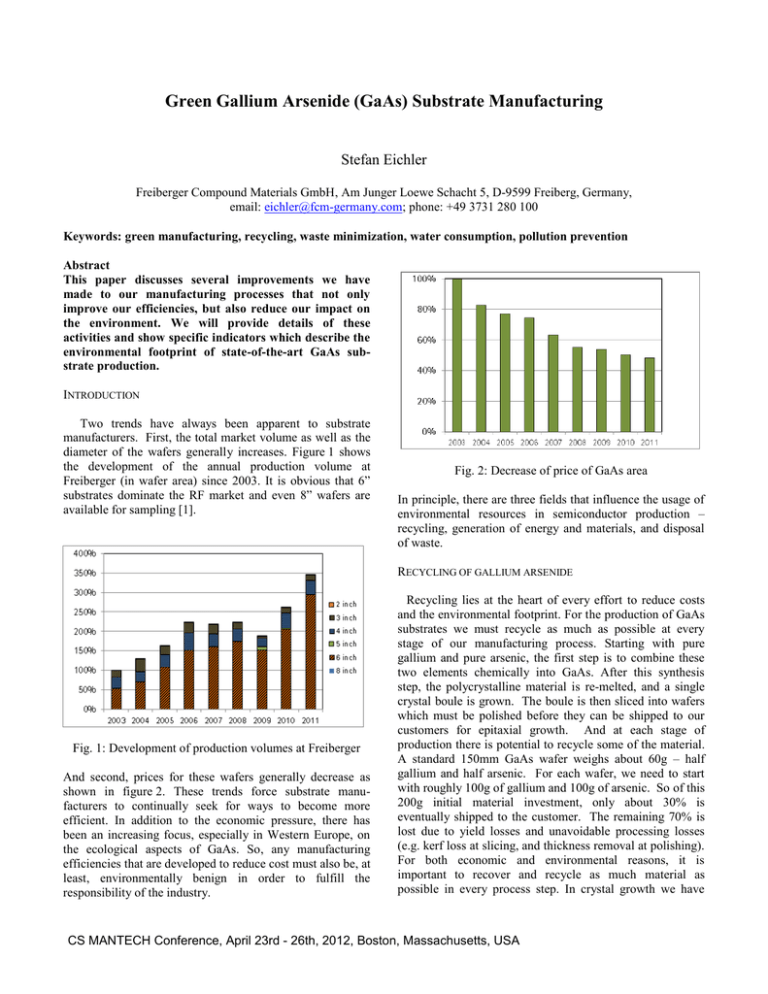
Green Gallium Arsenide (GaAs) Substrate Manufacturing Stefan Eichler Freiberger Compound Materials GmbH, Am Junger Loewe Schacht 5, D-9599 Freiberg, Germany, email: eichler@fcm-germany.com; phone: +49 3731 280 100 Keywords: green manufacturing, recycling, waste minimization, water consumption, pollution prevention Abstract This paper discusses several improvements we have made to our manufacturing processes that not only improve our efficiencies, but also reduce our impact on the environment. We will provide details of these activities and show specific indicators which describe the environmental footprint of state-of-the-art GaAs substrate production. INTRODUCTION Two trends have always been apparent to substrate manufacturers. First, the total market volume as well as the diameter of the wafers generally increases. Figure 1 shows the development of the annual production volume at Freiberger (in wafer area) since 2003. It is obvious that 6” substrates dominate the RF market and even 8” wafers are available for sampling [1]. Fig. 2: Decrease of price of GaAs area In principle, there are three fields that influence the usage of environmental resources in semiconductor production – recycling, generation of energy and materials, and disposal of waste. RECYCLING OF GALLIUM ARSENIDE Fig. 1: Development of production volumes at Freiberger And second, prices for these wafers generally decrease as shown in figure 2. These trends force substrate manufacturers to continually seek for ways to become more efficient. In addition to the economic pressure, there has been an increasing focus, especially in Western Europe, on the ecological aspects of GaAs. So, any manufacturing efficiencies that are developed to reduce cost must also be, at least, environmentally benign in order to fulfill the responsibility of the industry. Recycling lies at the heart of every effort to reduce costs and the environmental footprint. For the production of GaAs substrates we must recycle as much as possible at every stage of our manufacturing process. Starting with pure gallium and pure arsenic, the first step is to combine these two elements chemically into GaAs. After this synthesis step, the polycrystalline material is re-melted, and a single crystal boule is grown. The boule is then sliced into wafers which must be polished before they can be shipped to our customers for epitaxial growth. And at each stage of production there is potential to recycle some of the material. A standard 150mm GaAs wafer weighs about 60g – half gallium and half arsenic. For each wafer, we need to start with roughly 100g of gallium and 100g of arsenic. So of this 200g initial material investment, only about 30% is eventually shipped to the customer. The remaining 70% is lost due to yield losses and unavoidable processing losses (e.g. kerf loss at slicing, and thickness removal at polishing). For both economic and environmental reasons, it is important to recover and recycle as much material as possible in every process step. In crystal growth we have CS MANTECH Conference, April 23rd - 26th, 2012, Boston, Massachusetts, USA increased the share of recycled material by collecting all polycrystalline parts which are not contaminated by impurities. Another example of a recycling loop within a process step is the re-polishing of wafers which do not meet the prime specification after first polishing. And it is also possible to recover scrap material in one process step and use it in another one. So we clean broken wafers and add them to the material used for the single crystal growth process. For the internal recycling efficiency we define a key performance indicator: raw material yield (crystal mass divided by mass of virgin gallium and arsenic) minus crystal growth yield (crystal mass divided by total charge). Figure 3 shows the improvement of the internal recycling efficiency at Freiberger since 2003. wafer production line (synthesis and crystal growth) are very energy intensive. The melting point of GaAs is 1,238 degrees Celsius. So a large amount of heat must be first generated to melt the material and then be removed in a controlled fashion. The required heat is typically obtained using electrical furnaces, but electricity is usually generated from something else (coal, gas, oil, etc.). To reduce both costs and our environmental impact, we have built a cogeneration plant in our facility. Figure 4a shows the conventional energy supply scheme with which we used about 20 GWh/year electricity for production/media supply and cooling and 4 GWh/year gas for heating. Fig. 3: Increase of internal GaAs recycling efficiency When direct recycling is not possible, we at least try to recover and recycle the gallium contained in the scrap material. Despite we have minimized the amount of kerf loss by improving our wire sawing technology, there is still material lost with the slurry which we now recover in a special recycling procedure. Taking into account all external recycling, we recover nearly 50 % of the starting gallium. So, together with the about 30 % shipped to the customer, it is only the approximately 20 % that is lost during the damage etching and polishing processes which we cannot yet recover economically. Today we are working on new technologies to extract gallium and arsenic ions out of waste water and wet chemicals. ENERGY EFFICIENCY The preceding sections have discussed how recycling can influence the manufacturing cost of a GaAs wafer. Recycling however is not limited to the main raw materials. It also includes essential auxiliary and operating materials such as boron oxide, water and electricity and there are several further ways, in which both the costs and the environment can benefit. As an example, the initial steps in the GaAs Fig. 4 Scheme of power cogeneration plant After having implemented the co-generation plant (gas engines of 600 kW electrical power) we are now internally producing about 50 % of our electricity (9 GWh/year) (see figure 4b). And due to the utilization of waste heat in the power generation process for cooling in summer and heating in winter, the energy conversion efficiency is about 95%. For comparison, the conversion efficiency of a big state of the art power plant is between 40 % and 50 %. Thus, we have reduced the overall consumption of fossile fuel from 44 GWh/year to 38 GWh/year and the corresponding CO2 emissions by 11 % equaling 130 t/year. Due to increased CS MANTECH Conference, April 23rd - 26th, 2012, Boston, Massachusetts, USA charges in crystal growth, higher yields and the application of new energy efficient processes we have also improved our specific energy consumption. For example, the waste heat produced by the growth furnaces is now used in a heat exchanger for heating purposes. Figure 5 depicts the decrease of our specific consumption of electricity. wafer cleaning processes - like quick dump rinse - is even more pure than the incoming natural water which is normally laden with different types of ions. This amount of waste water is reintroduced with the raw water feed into the revers osmosis (RO) system. In addition for lower quality water requirements, such as for grinding processes, we have implemented closed cycles where we are concentrating the GaAs fraction for material recycling and reuse the water for processing again. In this case we have to replace only 2 % of the total stream with fresh water. The RO reject water of about 13 % is efficiently used for evaporation in cooling tower. The water balance of Freiberger is shown schematically in figure 7. Fig. 5 Specific electricity consumption (kWh/cm2) In addition to the energy gains described above, it has also been possible to improve the energy efficiency by higher fab utilization because of the fixed energy consumption of the fab systems. The corresponding development of the CO2 footprint is shown in figure 6. Fig. 7 Water balance (without cooling cycle) The development of the water consumption per produced wafer area is presented in figure 8. The difference between incoming natural water and outgoing waste water volumes corresponds to the amount of evaporated water for cooling purpose. Fig. 6 Specific CO2 footprint (kg/cm2) Altogether, this improvement in energy efficiency has enabled the company to compensate for the 100% energy price increase in Germany during the last decade. WATER MANAGEMENT Water consumption in the semiconductor industry in general is huge, and most of the water has to be of ultra high purity [2]. Beside the closed cycle of cooling water (600 m3/h) for the synthesis and crystal growth equipment, 26 % of the process water is recycled. Much of the waste water from the Fig. 8 Water consumption (l/cm2) In the EU, the pollution of waste water and waste air is restricted by law, and the waste treatment has to be able to CS MANTECH Conference, April 23rd - 26th, 2012, Boston, Massachusetts, USA fulfill these restrictions. In table I, the most important pollution values of Freiberger are compared with the statutory limits. By regular measurements it is proven that Freiberger easily fulfills all of the above pollution requirements. TABLE I Comparison of pollution values of Freiberger and corresponding legal limits Waste water pH value Arsenic Organohalogenids Chlorine VHH BTEX Air pollution Chlorine HCl Ammonia NOx Arsenic dust Freiberger’s emission/pollution Legal emission/pollution limits (EU) 8 0.1 mg/l 0.5 mg/l < 0.1 mg/l 0.05 mg/l < 0.05 mg/l 6.5 - 10 0.3 mg/l 0.5 mg/l 0.5 mg/l 0.1 mg/l 0.05 mg/l 0.5 kg/h 0.1 kg/h 0.1 kg/h 0.6 kg/h 0.0 mg/h 15 kg/h 0.15 kg/h 0.15 kg/h 1.8 kg/h 0.0001 mg/h DISPOSAL OF SOLID WASTE Most of the solid waste has to be landfilled. The metal hydroxide sludge from our water treatment is the dominating solid waste in our facility. All measures to decrease specific water consumption lead to a reduction of solid waste as well. If we compare the data of specific volume of solid waste as shown in figure 9 with the data of water consumption in figure 8, the same trend is visible. There are many other minor options to reduce the solid waste volume, for example use of state of the art data management systems to reduce paperwork, or implementation of advanced technologies to increase lifetime of supplies like polishing pads, crucibles and graphite parts. CONCLUSIONS In GaAs substrate manufacturing there are many opportunities to reduce the environmental footprint. Most of the measures also result in cost saving which is expected from the market. Sometimes the return of investment period is a bit above industry average but in the long run the environment will benefit. The most important strategies are to recycle as much as possible and use material, supplies and energy efficiently. The application of co-power generation requires a certain ratio of electricity consumption and heating/cooling demand. At Freiberger this ratio is very reasonable and we can reduce our environmental footprint even at the power generation stage. Generally this paper shows that Freiberger is continuously decreasing the environmental impact of GaAs wafer production. ACKNOWLEDGEMENTS The author would like to thank Dr. Russell E. Kremer and Claudia Paul for their help during the preparation of this paper and the whole team at Freiberger for the continuous support. REFERENCES [1] J. Stenzenberger et al., Journal of Crystal Growth 250 (2003) 57-61 [2] E. Burke, Waste Minimization, Pollution Prevention and Resource recovery at a GaAs Manufactuer, 2010 CS MANTECH Technical Digest, May 2010. ACRONYM Fig. 9 Development of specific volume of solid waste (g/cm2) CS MANTECH Conference, April 23rd - 26th, 2012, Boston, Massachusetts, USA

