Low Loss Thyristors for High Power Applications
advertisement

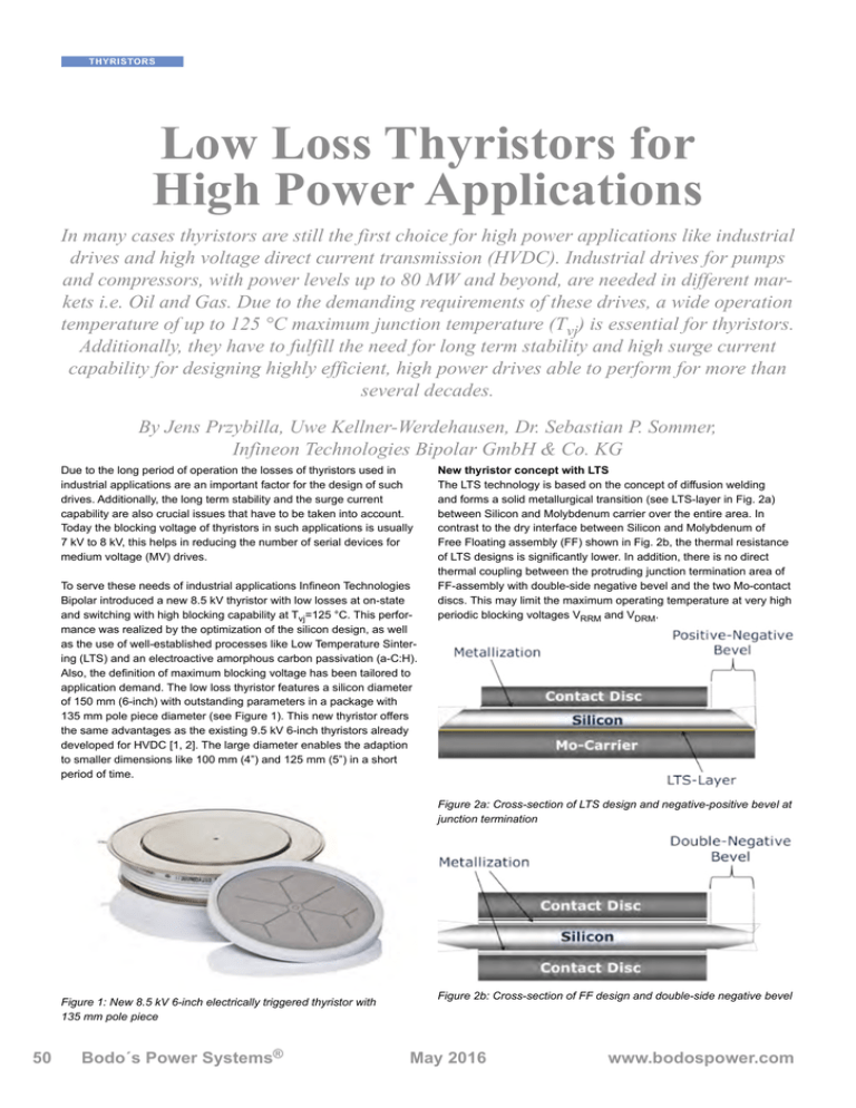
THYRISTORS CONTENT Low Loss Thyristors for High Power Applications In many cases thyristors are still the first choice for high power applications like industrial drives and high voltage direct current transmission (HVDC). Industrial drives for pumps and compressors, with power levels up to 80 MW and beyond, are needed in different markets i.e. Oil and Gas. Due to the demanding requirements of these drives, a wide operation temperature of up to 125 °C maximum junction temperature (Tvj) is essential for thyristors. Additionally, they have to fulfill the need for long term stability and high surge current capability for designing highly efficient, high power drives able to perform for more than several decades. By Jens Przybilla, Uwe Kellner-Werdehausen, Dr. Sebastian P. Sommer, Infineon Technologies Bipolar GmbH & Co. KG Due to the long period of operation the losses of thyristors used in industrial applications are an important factor for the design of such drives. Additionally, the long term stability and the surge current capability are also crucial issues that have to be taken into account. Today the blocking voltage of thyristors in such applications is usually 7 kV to 8 kV, this helps in reducing the number of serial devices for medium voltage (MV) drives. To serve these needs of industrial applications Infineon Technologies Bipolar introduced a new 8.5 kV thyristor with low losses at on-state and switching with high blocking capability at Tvj=125 °C. This performance was realized by the optimization of the silicon design, as well as the use of well-established processes like Low Temperature Sintering (LTS) and an electroactive amorphous carbon passivation (a-C:H). Also, the definition of maximum blocking voltage has been tailored to application demand. The low loss thyristor features a silicon diameter of 150 mm (6-inch) with outstanding parameters in a package with 135 mm pole piece diameter (see Figure 1). This new thyristor offers the same advantages as the existing 9.5 kV 6-inch thyristors already developed for HVDC [1, 2]. The large diameter enables the adaption to smaller dimensions like 100 mm (4”) and 125 mm (5”) in a short period of time. New thyristor concept with LTS The LTS technology is based on the concept of diffusion welding and forms a solid metallurgical transition (see LTS-layer in Fig. 2a) between Silicon and Molybdenum carrier over the entire area. In contrast to the dry interface between Silicon and Molybdenum of Free Floating assembly (FF) shown in Fig. 2b, the thermal resistance of LTS designs is significantly lower. In addition, there is no direct thermal coupling between the protruding junction termination area of FF-assembly with double-side negative bevel and the two Mo-contact discs. This may limit the maximum operating temperature at very high periodic blocking voltages VRRM and VDRM. Figure 2a: Cross-section of LTS design and negative-positive bevel at junction termination Figure 1: New 8.5 kV 6-inch electrically triggered thyristor with 135 mm pole piece 50 Bodo´s Power Systems® Figure 2b: Cross-section of FF design and double-side negative bevel May 2016 www.bodospower.com THYRISTORS CONTENT As a consequence, the better heat dissipation of LTS design leads to a higher maximum operating temperature of up to 125 °C. This has no negative effects on critical thyristor parameters like surge current or long term blocking voltage stability and periodic blocking voltage capability. By means of LTS the power loss during high reverse current flow, especially within junction termination, is sufficiently dissipated. For the new low loss concept described in this article the second option has been chosen reducing the silicon thickness by 6 percent in order to achieve significantly lower on-state voltage drop VT and dynamic losses, but without negative effect on the blocking capabilities. Table 1: Comparison of key parameters in LTS and FF design based on existing 4-inch devices [3, 4] Figure 3: Periodic blocking voltage and current at different operating temperatures using half sine wave of VRWM=7.5 kV superimposed by surge voltage up to VRRM=8.5 kV (tP=300 µs) It has already been reported that maximum periodic blocking voltage, VRRM and VDRM, can be further increased by 15 -20 percent without increasing the silicon wafer thickness. Testing was conducted according to standards (IEC 60747-6) for thyristors subjected to periodic voltage stress [2]. Typical current and voltage characteristics are shown in Figure 3. The half sine with tP=10 ms is applied with an amplitude equal to working voltage VRWM. This base sine wave is superimposed by surge voltage VRRM with higher amplitude during a shorter period of tP=300 µs. In this set-up the blocking current can reach values of several amps at very high voltages VDRM and VRRM. By introducing this Pulse Peak test concept two improvement options are possible: • Silicon thickness is kept constant, i.e. the same as existing thyristors, and VDRM/VRRM is increased. This leads to a significant reduction of the number of series connected devices and corresponding components, but without increased on-state losses. • Silicon thickness is reduced compared to existing thyristor, and VDRM/VRRM remains constant, but with significantly lower on-state voltage drop VT of single thyristor. www.bodospower.com Figure 4: Leakage current vs. operating temperature from periodic blocking voltage test using half sine wave (VRWM, VDWM=8.5 kV, tP=10 ms) tested on a typical device May 2016 Bodo´s Power Systems® 51 THYRISTORS CONTENT Device Performance Figure 3 depicts the periodic blocking test for a typical new low loss 6-inch device subjected to a periodic voltage stress at VRRM=8.5 kV and f=50 Hz. The recorded blocking voltage and leakage current waveforms were tested at four temperatures, 25 °C, 90 °C, 115 °C and 125 °C, respectively. Usually, the applied working voltage VRWM is between 60 and 80 percent of the peak voltage VRRM as recommended by different manufacturers [2, 5]. With the new concept, the selected VRWM applied is about 90 percent of the repetitive peak reverse blocking voltage VRRM. The new devices not only show an outstanding blocking capability, the losses of the thyristor have also been reduced significantly. In Figure 6 the reduction of losses are shown for a 150 mm silicon diameter amounting to approximately 30 percent lower switching losses. Compared to current designs, the reduced losses are caused by the recovery charge Qr, at the same on-state voltage vT. In Figure 4 the typical leakage current set against temperature behavior is shown. With this test the blocking performance of the new 8.5 kV low loss device is demonstrated for junction temperatures of up to 125 °C and frequency of 50 Hz. Figure 7: Calculated trade-off between reverse recovery charge Qr and on-state voltage drop VT of smaller 8.5 kV 6” thyristor with 100 mm pole piece using the defined conditions: IT=1.5 kA, di/dt=-1.5 A/µs, VR=-100 V In Figure 7 the calculated data for the new low loss thyristor with 100 mm silicon diameter is shown. For the defined conditions IT=1.5 kA, di/dt=-1.5 A/µs, VR=-100 V, the blocking capability of this smaller device will be as high performing as the 150 mm silicon diameter device. Figure 5: Leakage current vs. blocking voltage from Pulse Peak test (single pulse) at different temperatures and surge voltages (tP=300 µs) using half sine wave of VRWM=7.5 kV In addition, the peak voltage blocking performance is demonstrated in Figure 5. The device shows a capability of up to 9.5 kV peak blocking voltage at 125 °C. This data highlights the blocking margin of the new design enabling a long term blocking stability over decades. The key technologies for this margin are the LTS joining process and the bevel passivation process using an electroactive a-C:H layer. Figure 6: Qr vs. VT for existing and new low loss 8.5 kV 6-inch thyristor at operating temperature of 125 °C, derived from a few tested devices using IT=3 kA, di/dt=-1.5 A/µs, VR=-100 V Conclusion The article described a new 8.5 kV low loss thyristor family designed for industrial applications. With the new technology, full blocking capability at 50 Hz/60 Hz is achieved for 125 °C at 8.5 kV. Beside these key factors, outstanding surge current capability and low mechanical installation force are additional features of these devices which are important for industrial applications. This enables highly efficient and powerful applications with superior reliability for today´s and future´s demands. References [1] J. Przybilla, J. Dorn, R. Barthelmess, R. Joerke, U. KellnerWerdehausen, “Reaching New Limits with High Power Bipolar Devices”, Proceedings PCIM 2010, Nuremberg, pp. 761 – 766 [2] M. Schenk, J. Przybilla, U. Kellner-Werdehausen, R. Barthelmess, J. Dorn, G. Sachs, M. Uder, S. Völkel, „State of the Art of Bipolar Semiconductors for Very High Power Applications“, Proceedings PCIM Europe 2015, Nuremberg, pp. 930 – 936 [3] Datasheet “Infineon-T1901N-DS-v09_00-en_de”, www.Infineon. com [4] Datasheet “5STP 20N8500_5SYA1072-04 Dec 13”, http://new. abb.com/semiconductors [5] J. Vobecký, K. Stiegler, R. Siegrist, F. Weber, „Low Loss High Power Thyristors for Industrial Applications”, Bodo´s Power Systems, Nov. 2015, pp.18 – 21 www.infineon.com 52 Bodo´s Power Systems® May 2016 www.bodospower.com


