60 GHz VCO with Wideband Tuning Range Fabricated on VLSI SOI
advertisement
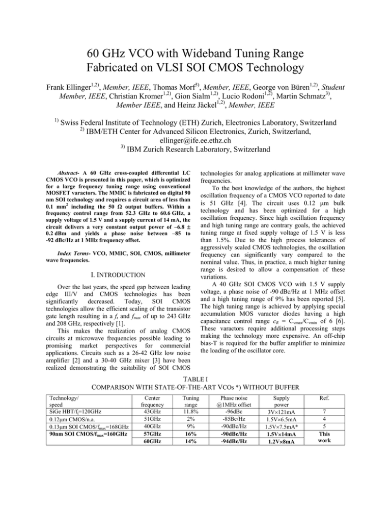
60 GHz VCO with Wideband Tuning Range Fabricated on VLSI SOI CMOS Technology Frank Ellinger1,2), Member, IEEE, Thomas Morf3), Member, IEEE, George von Büren1,2), Student Member, IEEE, Christian Kromer1,2), Gion Sialm1,2), Lucio Rodoni1,2), Martin Schmatz3), Member IEEE, and Heinz Jäckel1,2), Member, IEEE 1) Swiss Federal Institute of Technology (ETH) Zurich, Electronics Laboratory, Switzerland 2) IBM/ETH Center for Advanced Silicon Electronics, Zurich, Switzerland, ellinger@ife.ee.ethz.ch 3) IBM Zurich Research Laboratory, Switzerland Abstract- A 60 GHz cross-coupled differential LC CMOS VCO is presented in this paper, which is optimized for a large frequency tuning range using conventional MOSFET varactors. The MMIC is fabricated on digital 90 nm SOI technology and requires a circuit area of less than 0.1 mm2 including the 50 Ω output buffers. Within a frequency control range from 52.3 GHz to 60.6 GHz, a supply voltage of 1.5 V and a supply current of 14 mA, the circuit delivers a very constant output power of –6.8 ± 0.2 dBm and yields a phase noise between –85 to -92 dBc/Hz at 1 MHz frequency offset. Index Terms- VCO, MMIC, SOI, CMOS, millimeter wave frequencies. I. INTRODUCTION Over the last years, the speed gap between leading edge III/V and CMOS technologies has been significantly decreased. Today, SOI CMOS technologies allow the efficient scaling of the transistor gate length resulting in a ft and fmax of up to 243 GHz and 208 GHz, respectively [1]. This makes the realization of analog CMOS circuits at microwave frequencies possible leading to promising market perspectives for commercial applications. Circuits such as a 26-42 GHz low noise amplifier [2] and a 30-40 GHz mixer [3] have been realized demonstrating the suitability of SOI CMOS technologies for analog applications at millimeter wave frequencies. To the best knowledge of the authors, the highest oscillation frequency of a CMOS VCO reported to date is 51 GHz [4]. The circuit uses 0.12 µm bulk technology and has been optimized for a high oscillation frequency. Since high oscillation frequency and high tuning range are contrary goals, the achieved tuning range at fixed supply voltage of 1.5 V is less than 1.5%. Due to the high process tolerances of aggressively scaled CMOS technologies, the oscillation frequency can significantly vary compared to the nominal value. Thus, in practice, a much higher tuning range is desired to allow a compensation of these variations. A 40 GHz SOI CMOS VCO with 1.5 V supply voltage, a phase noise of -90 dBc/Hz at 1 MHz offset and a high tuning range of 9% has been reported [5]. The high tuning range is achieved by applying special accumulation MOS varactor diodes having a high capacitance control range cR = Cvmax/Cvmin of 6 [6]. These varactors require additional processing steps making the technology more expensive. An off-chip bias-T is required for the buffer amplifier to minimize the loading of the oscillator core. TABLE I COMPARISON WITH STATE-OF-THE-ART VCOs *) WITHOUT BUFFER Technology/ speed SiGe HBT/ft=120GHz 0.12µm CMOS/n.a. 0.13µm SOI CMOS/fmax=168GHz 90nm SOI CMOS/fmax=160GHz Center frequency 43GHz 51GHz 40GHz 57GHz 60GHz Tuning range 11.8% 2% 9% 16% 14% Phase noise @1MHz offset -96dBc -85Bc/Hz -90dBc/Hz -90dBc/Hz -94dBc/Hz Supply power 3V×121mA 1.5V×6.5mA 1.5V×7.5mA* 1.5V×14mA 1.2V×8mA Ref. 7 4 5 This work In this paper, a fully integrated 60 GHz SOI CMOS VCO is presented, which applies conventional MOSFET varactors. To allow process variations and high yield, the circuit is optimized for high frequency tuning range. Target applications are commercial wideband WLAN and optical transceivers operating around 60 GHz. Despite the high oscillation frequency, which to the best knowledge of the authors is the highest reported to date for a CMOS based oscillator, a high tuning range of more than 10 % is achieved with varactors having a cR of only 2. A comparison with recently reported silicon based VCOs is given in TABLE I. characteristic impedance of 95 Ω and an inductance of 0.9 nH/mm. For a line with length of 100 µm, an inductance of 90 pH and a quality factor of 20 at 60 GHz was extracted from measurements. Unfortunately, the used commercial VLSI process does not feature special varactor diodes with large tuning ranges as reported in [6]. However, the process provides thick oxide MOSFET capacitors allowing a CR of approximately 2 and quality factors around 5 at 60 GHz. The three top metals are used for the realization of the signal pads, which have a size of 54 µm x 50 µm. A low insertion loss of approximately 0.5 dB was measured at 60 GHz. II. TECHNOLOGY The VCO was fabricated using a 90 nm IBM VLSI SOI CMOS technology featuring a metal stack with 8 metal layers. A thin isolation layer between the active region and the substrate allows a relatively high substrate resistivity of 13.5 ± 5 Ωcm without increasing the threshold voltages Vth of the FETs required for digital applications. Thus, relatively high Q factors and operation frequencies can be achieved for the passive devices, which are mandatory for analog applications and oscillators. The possibility of highly integrated single chip solutions makes this technology well suited for future commercial applications. II. CIRCUIT DESIGN The circuit was simulated using SOI BSIM FET large signal models, and lumped equivalent circuits for the inductive lines, varactors, interconnects and pads. The applied software tool is Cadence. VDD Rdc1 LR LR Vtune Cv Cv wb wb Out A. FETs wo wo In Fig. 1, the simplified small signal equivalent circuit of a typical n-channel FET is shown. The device with Vth of 0.25 V and gate width w of 16 µm is biased in class A operation yielding a ft and fmax of approximately 150 GHz and 160 GHz, respectively, for the experimental hardware. G Cgd D Cgs gmVgs Rds Rgs Cds Cgs Rgs Cgd gm Rds Cds 22.5fF 56Ω 7.5fF 20.5mS 300Ω 3.75fF S Fig. 1. Simplified small signal equivalent circuit of MOSFET with w = 16 µm at Vgs = 0.5V, Vds = 1V and Ids = 4mA. B. Passive devices The upper copper metal is used for the realization of the inductive transmission lines. It has the largest distance to the lossy substrate and the highest metal thickness, which are approximately 7 µm and 1 µm, respectively. The line width is 4 µm yielding a Out Rb wdc Rb Rdc2 Fig. 2. Simplified VCO circuit schematics, Cvar = [25-50fF], LR = 90nH, wo = wb = 16µm, wdc = 32µm, Rb = 75µm, Rdc1 = 1.4kΩ, Rdc1 = 2kΩ. The simplified circuit schematics of the crosscoupled differential LC oscillator is shown in Fig. 2. A common drain output buffer is used since it has a high input and low output impedance thereby minimizing the loading of the oscillator core and allowing 50 Ω output matching. A voltage divider generates the required Vgs of the current source transistor. The frequency tuning range of the circuit is given by 1 1 ∆ω = − (1) LR Cv min + C p LR Cv max + C p ( ) ( ) with C p = Co,in + Co,out + Cb,in + CL (2) oscillation frequency of 60 GHz, which is still very high for a CMOS VCO. A photograph of the compact MMIC is shown in Fig. 3. The overall chip size is 0.3 mm × 0.25 mm. III. RESULTS 65 3.5 60 2.5 55 1.5 50 0.5 Vdd=1.2V Vdd=1.5V 45 40 -1.5 0.5 Out GND Out 1.5 2 2.5 3 3.5 Fig. 4. Measured frequency tuning range and varactor potential versus tuning voltage. LR GND 1 Vtune [V] Circuit core Vtune -0.5 Varactor potential [V] Measurements were performed on-wafer using an HP 8565E spectrum analyzer and an HP11974V preselected mixer. Oscillation frequency [GHz] as the total load of the oscillator core mainly consisting of the input and output capacitance of the oscillator core transistors Co,in and Co,out, the input capacitance of the buffer transistor Cb,in and the parasitic capacitance of the inductive line CL. To reach a high frequency control range, large varactor and small transistor sizes have to be chosen. However, decreasing of the oscillator transistor size wo lowers the gm required to compensate the losses of the resonator. This limits the maximum oscillation frequency since the losses increase with frequency. The minimum size of the buffer transistor wb is determined by the output power of the oscillator core. Consequently, the transistor and varactor sizes were optimized to ensure oscillation up to 65 GHz and to reach a frequency tuning range of more than 10%. With values of Co,in ≈ 25 fF, Cb,out ≈ 3.75 fF, Co,out ≈ 10 fF, CL ≈ 3 fF, LR = 90 pH, Cvmin = 25 fF and Cvmax = 50 fF, a tuning range from 55.4 GHz to 64.9 GHz can be calculated from Eqs. (1) and (2). VDD A. Tuning range The high tuning range of the circuit of 55.562.9 GHz and 52.3-60.6 GHz at supply voltages of Vdd = 1.2 V and Vdd = 1.5 V, respectively are shown in Fig. 4 including the effective varactor potential. The corresponding supply currents are 8 mA and 14 mA, respectively. The achieved tuning range agrees well with the theoretical considerations made in Section II. Fig. 3. Photograph of the VCO chip with overall size of 0.3 mm × 0.25 mm. Output power [dBm] Higher oscillation frequencies are possible by proper downscaling of CV, Lr and wo. We assume that wb can not be decreased due to large signal constraints. The decrease of wo and Lr is limited since the elements determine the loop gain required for loss compensation and stable oscillation. A significant increase of the oscillation frequency can be achieved by decreasing of CV. Unfortunately, this decreases the frequency tuning range as indicated in Eq. (1). For a frequency tuning range of 2 % and 0%, maximum oscillation frequencies of approximately 76 GHz and 80 GHz, respectively, would be possible. This is a interesting insight concerning the exploration of this technology and topology towards highest frequencies. However, in practice, this tuning range would be too small to compensate significant process variations thereby limiting the yield. Consequently, to have a reasonable tolerance margin, the circuit was optimized for a lower 0 -5 -10 -15 -20 Vdd=1.2V Vdd=1.5V -25 -30 0.5 1 1.5 2 2.5 3 3.5 Vtune [V] Fig. 5. Measured output power versus tuning voltage. B. Output power The measured output power versus tuning voltage is illustrated in Fig. 5. The losses of the cables and the RF probe were taken into account. A very constant output power of –6.8 ± 0.2 dBm was measured at Vdd = 1. 5V. An output power between –14 to -18.5 dBm was measured at the lower bias with Vdd = 1.2V. C. Phase noise A typical output spectrum is depicted in Fig. 6. At Vdd = 1.2 V and a frequency of approximately 60 GHz, a phase noise of –94 dBc/Hz was measured. excellent tuning range of higher than 10% has been achieved with conventional MOSFET varactors. Due to the high tuning range, the circuit allows a compensation of strong process variations, which is important for aggressively scaled CMOS technologies. Furthermore, the circuit has low phase noise, a compact size and a moderate power consumption. Thus, the VCO is well suited for commercial applications operating in accordance to future WLAN and optical transceivers. ACKNOWLEDGEMENTS L(1MHz) = (-39 -55) dBc/Hz = -94 dBc/Hz The authors would like to acknowledge Dr. C. Menolfi, Dr. M. Kossel and Dr. T. Toifl, all with IBM Research, Zurich Research Laboratory, for sharing their excellent expertise concerning the used technology and design environment. Furthermore, the author would like to thank H. Benedikter, IFH, for his help concerning millimeter wave measurements and for providing measurement equipment. REFERENCES Fig. 6. Measured output spectrum at 59.9 GHz, L: phase noise Vdd = 1.2V and Vtune = 2V. The measured phase noise at 1 MHz versus tuning range is shown in Fig. 7. Within the full tuning range, the phase noise is less than -85 dBc/Hz, which is sufficient for many applications. Phase noise [dBc/Hz] -80 -85 Vdd=1.2V Vdd=1.5V -90 -95 -100 0.5 1 1.5 2 2.5 3 3.5 Vtune [V] Fig. 7. Measured phase noise at 1 MHz offset versus tuning voltage. IV. CONCLUSION A 60 GHz SOI CMOS VCO has been presented in this paper. Despite this high oscillation frequency, which to the best knowledge of the authors is the highest reported to date for a CMOS oscillator, an [1] N. Zamdmer, J. Kim, R. Trzcinski, J.-O. Plochart, S. Narasimha, M. Khare, L. Wagner, S. Chaloux, "A 243GHz Ft and 208-GHz Fmax, 90-nm SOI CMOS SoC technology with low-power millimeter-wave digital and RF circuit capability", submitted to IEEE VLSI Technology 2004. [2] F. Ellinger, "26-42 GHz low noise amplifier MMIC fabricated on digital SOI CMOS technology ", accepted for publication in IEEE Journal of Solid-State Circuits. [3] F. Ellinger, L. C. Rodoni, G. Sialm, C. Kromer, G. von Büren, M. Schmatz, C. Menolfi, T. Toifl, T. Morf, M. Kossel, H. Jäckel, "30-40 GHz drain pumped passive down mixer MMIC fabricated on digital SOI CMOS technology", submitted to IEEE Transactions on Microwave Theory and Techniques. [4] M. Tiebout, H.-D. Wohlmuth and W. Simbürger, "A 1V 51 GHz fully-integrated VCO in 0.12 um CMOS", IEEE International Solid-State Circuits Conference, pp. 300301, Feb. 2002 [5] N. Fong, J.-O. Plouchart, N. Zamdmer, Liu Duixian, L. Wagner, P. Garry, G. Tarr, "A 40 GHz VCO with 9 to 15% tuning range in 0.13 µm SOI CMOS", Symposium on VLSI Circuits Digest, pp. 186-189, June 2002. [6] N. Fong, G. Tarr, N. Zamdmer, J.-O. Plouchard, C. Plett, "Accumulation MOS varactors for 4 to 40 GHz VCOs in SOI CMOS", IEEE International SOI Conference, pp. 158-160, Oct. 2002. [7] D. K. Schaeffer and S. Kudszus, "Performance-optimized microstrip coupled VCOs for 40-GHz and 43-GHz OC768 optical transmission", IEEE Journal of Solid-State Circuits, Vol. 38, No. 7, July 2003.
