Feedback Amplifiers
advertisement

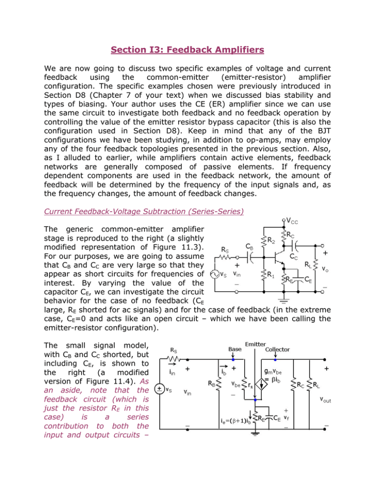
Section I3: Feedback Amplifiers We are now going to discuss two specific examples of voltage and current feedback using the common-emitter (emitter-resistor) amplifier configuration. The specific examples chosen were previously introduced in Section D8 (Chapter 7 of your text) when we discussed bias stability and types of biasing. Your author uses the CE (ER) amplifier since we can use the same circuit to investigate both feedback and no feedback operation by controlling the value of the emitter resistor bypass capacitor (this is also the configuration used in Section D8). Keep in mind that any of the BJT configurations we have been studying, in addition to op-amps, may employ any of the four feedback topologies presented in the previous section. Also, as I alluded to earlier, while amplifiers contain active elements, feedback networks are generally composed of passive elements. If frequency dependent components are used in the feedback network, the amount of feedback will be determined by the frequency of the input signals and, as the frequency changes, the amount of feedback changes. Current Feedback-Voltage Subtraction (Series-Series) The generic common-emitter amplifier stage is reproduced to the right (a slightly modified representation of Figure 11.3). For our purposes, we are going to assume that CB and CC are very large so that they appear as short circuits for frequencies of interest. By varying the value of the capacitor CE, we can investigate the circuit behavior for the case of no feedback (CE large, RE shorted for ac signals) and for the case of feedback (in the extreme case, CE=0 and acts like an open circuit – which we have been calling the emitter-resistor configuration). The small signal model, with CB and CC shorted, but including CE, is shown to the right (a modified version of Figure 11.4). As an aside, note that the feedback circuit (which is just the resistor RE in this case) is a series contribution to both the input and output circuits – hence the series-series designation I confused the mess out of you with in the previous section. Anyway, using the small signal circuit, we can see that the output voltage is v out = − β ib (RC || RL ) , while the input voltage (note that the voltage across RB is vin, so we don’t need to include it in the equation) is v in = i b rπ + β i b (RE || Z CE ) = β i b [re + (RE || Z CE )] , where the impedance of the capacitor, CE, is defined as ZCE=1/sCE and we have assumed that (β+1)≈β. The voltage gain of the common-emitter stage now becomes a function of frequency and is given by Av = v out = v in − βi b (RC || RL ) ⎡ ⎞⎤ βi b ⎢re + ⎛⎜ RE || 1 ⎟⎥ sC E ⎠⎦ ⎝ ⎣ = − (RC || RL ) ⎞ re + ⎛⎜ RE || 1 ⎟ sC E ⎠ ⎝ . (Equation 11.4) We can look at the two feedback extremes by making appropriate modifications to the capacitor impedance in Equation 11.4. The voltage gain with maximum feedback (i.e., the emitter-resistor configuration) is known as the closed-loop gain and is found by letting CE go to zero or equivalently, letting ZCE go to infinity (an open circuit), in Equation 11.4. The expression for the closed-loop gain then becomes Av (closed loop) = − (RC || RL ) re + RE , (Equation 11.5, Modified) which is just the gain expression for the emitter-resistor configuration. Note that your author has further simplified this relationship in the text version of Equation 11.5 by letting RE >> re. While this may be true most of the time, I don’t really want to make a firm commitment – if it is true, it will be obvious and fall out in the math. Similarly, the voltage gain without feedback (i.e., the common-emitter configuration) is designated the open-loop gain and is found by letting CE go to infinity or equivalently, letting ZCE go to zero (a short circuit), in Equation 11.4. If ZCE is zero, the parallel combination of RE and ZCE is also zero and the open-loop gain is Av (open loop) = − β (RC || RL ) − (RC || RL ) = −g m (RC || RL ) = rπ re , (Equation 11.6) which is the gain expression for the common-emitter amplifier. A couple of things to notice from Equations 11.4, 11.5 and 11.6: ¾ The closed-loop gain is much smaller than the open-loop gain since re+RE>> re. ¾ If RE >> re, the closed-loop gain expression does not include any transistor parameter values and the gain depends only on the ratio of external components. Contrast this with the open-loop gain (without feedback) that is dependent on the transistor parameters β and rπ. ¾ Equation 11.4 is the most general form of closed-loop gain with feedback, where the amount of feedback depends on the frequency of operation (through the impedance of the capacitor). Recall that the closed-loop transfer function of the model in the previous section was given by G(s) = G o (s) 1 + G o (s)H(s) , (Equation 11.3) where Go(s) was the open loop transfer function and H(s) was defined as the feedback factor. Associating parameters in the above expression with Equations 11.5 (or 11.4) and 11.6, we have G(s) = Av (closed loop) = Av G o (s) = Av (open loop) = Avo , where the frequency dependence is implied and the terms Av and Avo have been introduced to save typing (or writing). Rearranging Equation 11.4 (the most general feedback representation) to fit the form of Equation 11.3, we get Av = Avo ⎞ ⎛ ⎟ ⎜ ⎟ ⎛ − (RC || RL ) ⎞⎜ 1 1 ⎟⎟⎜ = ⎜⎜ ⎟ re 1 + Avo H ⎝ ⎛ − (RC || RL ) ⎞⎛ − (RE || Z CE ) ⎞ ⎟ ⎠⎜ ⎜ ⎟⎟⎜⎜ ⎟⎟ ⎟ ⎜1 + ⎜ re ⎝ ⎠⎝ RC || RL ⎠ ⎠ . ⎝ Prove to yourself that this actually works! The reason we’re making such a nice equation look so incredibly ugly is so we can pick off the term that corresponds to H(s), or − (RE || Z CE ) = H(s) = RC || RL ⎞ − ⎛⎜ RE || 1 ⎟ sC E ⎠ ⎝ RC || RL . (Equation 11.11) Note that your author refers to H(s) as the feedback attenuation factor γ (also called β in many references) and defines this feedback factor in terms of the feedback voltage, Vf, to be γ = − (RE || Z CE ) Vf = v out RC || RL . (Equation 11.11) Using the expression for vout, we can express the feedback voltage in terms of the collector current (remember we’re assuming (β+1)≈β so ie≈ic=βib) and the equivalent impedance in the emitter circuit as Vf = βi b (RE || Z CE ) , which is the same quantity that reduces vbe observed in the KVL of the baseemitter loop of Figure 11.4, or v be = v in − i e (RE || Z CE ) ≅ v in − βi b (RE || Z CE ) = v in − Vf . Finally, we can express the general expression of gain with feedback found in Equation 11.4 in the form of Equation 11.3 as Av = Avo 1 + γAvo ! (Equation 11.12) Notice that since both γ and Avo are negative, the loop gain γAvo is positive – as it must be for negative feedback! The sensitivity of an amplifier to changes in gain is determined by differentiating Equation 11.12 with respect to Avo, or dAvo dAv 1 = ; or dAV = 2 dAvo (1 + γAvo ) (1 + γAvo )2 . (Equation 11.13, Modified) Dividing both sides by Av (as given in Equation 11.12), Equation 11.13 becomes ⎛ dAvo dAv =⎜ ⎜ (1 + γA )2 Av vo ⎝ ⎞⎛ 1 + γAvo ⎟⎜ ⎟⎜⎝ Avo ⎠ ⎞ dAvo dAvo ⎟⎟ = ≈ 2 ⎠ Avo (1 + γAvo ) γAvo , (Equation 11.14) where the last approximation was made by assuming that γAvo >> 1. OK, great, what does this tell us? The ratio on the left hand side (dAv/Av) represents the variation in closed loop gain with respect to the nominal closed-loop gain value. The ratio on the (far) right hand side indicates that this is approximately equal to the change in open loop gain divided by γ(Avo)2. Since γ(Avo)2 is usually quite large, we can see that the variation in closed-loop gain is greatly reduced for a given variation in open-loop gain, or the closed loop gain becomes insensitive to changes in open loop gain. Now, wasn’t that worth it? Voltage Feedback-Current Subtraction (Shunt-Shunt) The other form of feedback that we will be explicitly looking at was also introduced in Section D8 and is shown in Figure 11.5a (reproduced to the right). Here, we have replaced the R1R2 combination that formed the base resistor, RB, under ac conditions with a feedback resistor, RF, which is tied between the base and collector of the BJT. For this form of feedback, the resistor RF “samples” the output voltage vO and feeds back a current that is then mixed with the source current. Since vo > vin, the current will flow as indicated in the figure above. For our purposes, we will assume that the capacitors CC and CE are sufficiently large so that they become short circuits at frequencies of interest. It appears that your author has renamed vsource as vin in Figures 11.5a and 11.5b – I’m not sure why, but this is not valid unless RS is equal to zero. The resulting gain equations will be in the form of vo/vS instead of vo/vin. If vo/vin is desired, the input voltage divider will be required. The small signal circuit to the right contains the same information as Figure 11.5b in your text, but seems to be to be more in line visually with what we’ve been doing so far. Writing a KCL at the base node, ib = iS + if = v S − vπ v − vπ + o RS RF = ⎛ 1 vS v 1 ⎞ ⎟ + o − v π ⎜⎜ + RS RF RF ⎟⎠ ⎝ RS = vS v vπ + o − RS RF RS || RF Since ib is also equal to vπ/rπ, we may rewrite the above equation as ⎛ ⎞ vS rπ v v v i b rπ ⎟⎟ = ib = S + o − ; i b ⎜⎜1 + + o ; ib = RS || RF ⎠ RS RF RS RF RS || RF ⎝ α ≡1+ rπ RS || RF . vS RS + vo RF α , where (Equation 11.18) Expressing the output voltage in terms of the base current as v out = − βib (RC || RL ) , and after much algebra (that I will provide if requested), the expression of Equation 11.19 is reached. I want to stress again that this relationship is a general expression of closed loop gain, but is in terms of vo/vS NOT vo/vin. This is an acceptable strategy since the difference between the two is a resistive voltage divider that we are assuming is not frequency dependent, but be sure you know what you are actually calculating! − β (RC || RL ) vo αRS Av = = β (RC || RL ) vS 1+ α RF . (Equation 11.19, Modified) To find the open-loop gain expression, let RF→∞ so that α=1+rπ/RS. Avo = − β (RC || RL ) RS + rπ . (Equation 11.20) Following the same strategy as the earlier discussion, we can rewrite Equation 11.19 in the form of Equation 11.3 as Av = Avo Avo = − RS ⎞ 1 + γAvo 1 + Avo ⎛⎜ ⎟ R F ⎠ ⎝ , (Equation 11.21) where γ = −RS / RF . Again, note that both γ and Avo are negative so that the loop gain γAvo is positive and the closed-loop gain is less than the open-loop gain. Also, as Avo becomes large, Av approaches 1/γ=-RF/RS, which is independent of transistor parameters.


