Parameter Subclause reference Value Units Differential peak
advertisement

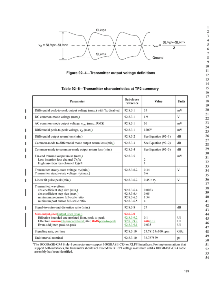
SLi<p> vdi = SLi<p>SLi<n> vcmi = SLi<n> SLi<p>+SLi<n> 2 Ground Figure 92–4—Transmitter output voltage definitions Table 92–6—Transmitter characteristics at TP2 summary Parameter Subclause reference Value Units Differential peak-to-peak output voltage (max.) with Tx disabled 92.8.3.1 35 mV DC common-mode voltage (max.) 92.8.3.1 1.9 V AC common-mode output voltage, vcmi (max., RMS) 92.8.3.1 30 mV Differential peak-to-peak voltage, vdi (max.) 92.8.3.1 1200a mV Differential output return loss (min.) 92.8.3.2 See Equation (92–1) dB Common-mode to differential mode output return loss (min.) 92.8.3.3 See Equation (92–2) dB Common-mode to common-mode output return loss (min.) 92.8.3.4 See Equation (92–3) dB Far-end transmit output noise (max.) Low insertion loss channel Txfel High insertion loss channel Txfeh 92.8.3.5 Transmitter steady-state voltage, vf (min.) Transmitter steady-state voltage, vf (max.) 92.8.3.6.2 0.34 0.6 V Linear fit pulse peak (min.) 92.8.3.6.2 0.45 × vf V Transmitted waveform abs coefficient step size (min.) abs coefficient step size (max.) minimum precursor full-scale ratio minimum post cursor full-scale ratio 92.8.3.6.4 92.8.3.6.4 92.8.3.6.5 92.8.3.6.5 0.0083 0.05 1.54 4 Signal-to-noise-and-distortion ratio (min.) 92.8.3.8 27 dB Max output jitterOutput jitter (max.) Effective bounded uncorrelated jitter, peak-to-peak Effective randomtotal uncorrelated jitter, RMSpeak-to-peak Even-odd jitter, peak-to-peak 92.8.3.9 92.8.3.9.2 92.8.3.9.2 92.8.3.9.1 0.1 0.010.18 0.035 UI UI UI Signaling rate, per lane 92.8.3.10 25.78125±100 ppm GBd Unit interval nominal 92.8.3.10 38.787879 ps mV 2 1 aThe 100GBASE-CR4 Style-1 connector may support 100GBASE-CR4 or XLPPI interfaces. For implementations that support both interfaces, the transmitter should not exceed the XLPPI voltage maximum until a 100GBASE-CR4 cable assembly has been identified. 199 1 2 3 4 5 6 7 8 9 10 11 12 13 14 15 16 17 18 19 20 21 22 23 24 25 26 27 28 29 30 31 32 33 34 35 36 37 38 39 40 41 42 43 44 45 46 47 48 49 50 51 52 53 54 0 Meets equation constraints Insertion Loss (dB) 5 10 15 20 25 30 0 2 4 6 8 10 12 14 16 18 20 Frequency (GHz) Figure 92–7—Maximum insertion loss TP0 to TP2 or TP3 to TP5 92.8.3.8 Transmitter output noise and distortion Signal-to-noise-and-distortion ratio (SNDR) is measured at the transmitter output using the following method. Given a configuration of the transmit equalizer, capture at least one complete cycle of the test pattern PRBS9 as specified in 83.5.10 at TP0a per 85.8.3.3.4. Compute the linear fit pulse response p(k) and the linear fit error waveform e(k) from the captured waveform per 85.8.3.3.5 using Np = 14 and Dp = 2. Denote the standard deviation of e(k) as e. Given the same configuration of the transmit equalizer, measure the RMS deviation from the mean voltage at a fixed point in a run of at least 8 consecutive identical bits in a suitable pattern. PRBS9 is an example of a pattern that includes runs suitable to perform the measurement. It is recommended that the deviation is measured within the flattest portion of the waveform at a point where the slope is closest to zero. The RMS deviation is measured for a run of zeros and also a run of ones. The average of the two measurements is denoted as n. SNDR is defined by Equation (92–1) where pmax is the maximum value of p(k). 2 p max - dB SNDR = 10log 10 ----------------2 2 e + n (92–1) SNDR shall be greater than 27 dB regardless of the transmit equalizer setting. 92.8.3.9 Transmitter output jitter Three components of the transmitter output jitter are definedspecified in this subclause: even-odd jitter, effective bounded uncorrelated jitter, and effective randomtotal uncorrelated jitter. The effect of a single-pole high-pass filter with a 3 dB frequency of 10 MHz is applied to the jitter. The voltage threshold for the measurement of BER or crossing times is the mid-point (0 V) of the AC-coupled differential signal. 205 1 2 3 4 5 6 7 8 9 10 11 12 13 14 15 16 17 18 19 20 21 22 23 24 25 26 27 28 29 30 31 32 33 34 35 36 37 38 39 40 41 42 43 44 45 46 47 48 49 50 51 52 53 54 1 2 3 4 5 6 7 8 9 10 11 12 13 14 15 16 17 18 19 20 21 22 23 24 25 26 27 28 29 30 31 32 33 34 35 36 37 38 39 40 41 42 43 44 45 46 47 48 49 50 51 52 53 54 92.8.3.9.1 Even-odd jitter Even-odd jitter is measured on two repetitions of a repeating pattern with an odd number of bits and at least two transitions between one and zero or zero and one. PRBS9 is such a pattern. The deviation of the time of each transition from an ideal clock at the signaling rate is measured. Even-odd jitter is defined as the magnitude of the difference between the average deviation of all even-numbered transitions and the average deviation of all odd-numbered transitions, where determining if a transition is even or odd is based on possible transitions but only actual transitions are measured and averaged. Even-odd jitter shall be less than or equal to 0.035 UI regardless of the transmit equalization setting. NOTE—Even-odd jitter has been referred to as duty cycle distortion by other Physical Layer specifications for operation over electrical backplane or twinaxial copper cable assemblies (see 72.7.1.9). The term even- odd jitter is used here to distinguish it from the duty cycle distortion referred to by Physical Layer specifications for operation over fiber optic cabling. 92.8.3.9.2 Effective bounded uncorrelated jitter and effective random jitter Effective bounded uncorrelated jitter and effective random jitter are measured on each of two specific transitions in a PRBS9 pattern (see 83.5.10). The two transitions occur in the sequence of five zeros and four ones and nine ones and five zeros, respectively. The sequences are located at bits 10 to 18 and 1 to 14, respectively, where bits 1 to 9 are the run of nine ones. The jitter components are determined according to the following method. a) b) c) d) e) 206 Acquire a horizontal histogram of a transition around the zero-crossing point. The number of acquired samples should be sufficiently large to yield consistent measurement results. Acquire a horizontal histogram with at least 20 000 samples of a transition measured at the zero crossing point, with resolution no coarser than 20 fs per bin and with vertical size of the histogram box no more than 1 % of the signal VMA (see 86A.5.3.5). Designate the total number of samples as NS, the number of bins as NB, the number of samples perin each bin as Ni where i is the bin number from 1 to NB, and the sample time corresponding with the center of each bin as ti. Create two cumulative distribution curves CDFLi and CDFRi according to Equation (92–11) and Equation (92–12) and two corresponding curves QRi and QLi according to Equation (92–13) and Equation (92–14), where erfc–1(x) is the inverse of the complementary error function erfc(x) defined by Equation (92–15). Determine the bin numbers IL1, IL2, IR1, and IR2 meeting the following criteria: CDFLIL1>=20/NS and CDFLIL1-1<20/NS, CDFLIL2<=500/NS and CDFLIL2+1>=500/NS, CDFRIR1>=20/NS and CDFRIR1+1<20/NS, and CDFRIR2<=500/NS and CDFRIR2-1>=500/NS. Determine a straight line fit to QRi and QLi versus ti for i over the ranges IL1 to IL2 and IR1 to IR2 and of the forms in Equation (92–16) and Equation (92–17), respectively.Determine the parameters mleft and bleft of Equation (92-16) that best fit QLi as a function of ti for bins with CDFLi in the range of 10–3 to 2.5 × 10⁻². Similarly determine the parameters of mright and bright that best fit QRi as a function of ti for bins with CDFRi in the range of 10–3 to 2.5 × 10⁻². Calculate the values of effective bounded uncorrelated jitter and effective randomtotal uncorrelated jitter according to Equation (92–18) and Equation (92–21), respectively. The peak-to-peak contribution of the effective random jitter in the effective total uncorrelated jitter is related to a bit error ratio of 10–5. i CDFL i = k=1 NB CDFR i = N ------kNS Nk (92–11) -----NS (92–12) –1 (92–13) –1 (92–14) k=i QL i = 2 erfc 2 CDFL i QR i = 2 erfc 2 CDFR i 2 2 –t erfc x = ------- e dt (92–15) Q left = m left t + b left (92–16) Q right = m right t + b right (92–17) effective bounded uncorrelated jitter = EBUJ = b left m left – b right m right (92–18) effective random jitter = ERJ = 2 m right – m left (92–19) m left – m right effective random jitter = ERJ = --------------------------------2 m right m left (92–20) effective total uncorrelated jitter = 7.9 ERJ + EBUJ (92–21) x Effective bounded uncorrelated jitter shall be less than or equal to 0.1 UI peak-to-peak regardless of the transmit equalization setting. The effective randomtotal uncorrelated jitter shall be less than or equal to 0.010.18 UI RMSpeak-to-peak regardless of the transmit equalization setting. 92.8.3.10 Signaling rate range The 100GBASE-CR4 MDI signaling rate shall be 25.78125 GBd ±100 ppm per lane. The corresponding unit interval is approximately 38.787879 ps. 92.8.4 Receiver characteristics The receiver characteristics are summarized in Table 92–7. Unless specified otherwise, all receiver measurements defined in Table 92–7 are made at TP3 utilizing the test fixtures specified in 92.11.1. Unless otherwise specified, a test system with a fourth-order Bessel-Thomson low-pass response with 33 GHz 3 dB bandwidth is to be used for all receiver input signal measurements. The receiver specifications at TP5 are provided informatively in Annex 92A. 92.8.4.1 Receiver input amplitude tolerance 100GBASE-CR4 receiver shall operate at a BER better than 10–5 when connected to a compliant transmitter whose peak-to-peak differential output voltage, as defined by 92.8.3.1 using preset equalizer coefficients, is 207 1 2 3 4 5 6 7 8 9 10 11 12 13 14 15 16 17 18 19 20 21 22 23 24 25 26 27 28 29 30 31 32 33 34 35 36 37 38 39 40 41 42 43 44 45 46 47 48 49 50 51 52 53 54


