A 12 Gb/s Chip-to-Chip AC Coupled Transceiver
advertisement

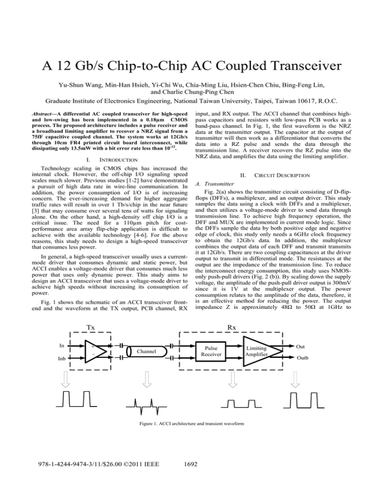
A 12 Gb/s Chip-to-Chip AC Coupled Transceiver Yu-Shun Wang, Min-Han Hsieh, Yi-Chi Wu, Chia-Ming Liu, Hsien-Chen Chiu, Bing-Feng Lin, and Charlie Chung-Ping Chen Graduate Institute of Electronics Engineering, National Taiwan University, Taipei, Taiwan 10617, R.O.C. Abstract—A differential AC coupled transceiver for high-speed and low-swing has been implemented in a 0.18µm CMOS process. The proposed architecture includes a pulse receiver and a broadband limiting amplifier to recover a NRZ signal from a 75fF capacitive coupled channel. The system works at 12Gb/s through 10cm FR4 printed circuit board interconnect, while dissipating only 13.5mW with a bit error rate less than 10-12. I. INTRODUCTION Technology scaling in CMOS chips has increased the internal clock. However, the off-chip I/O signaling speed scales much slower. Previous studies [1-2] have demonstrated a pursuit of high data rate in wire-line communication. In addition, the power consumption of I/O is of increasing concern. The ever-increasing demand for higher aggregate traffic rates will result in over 1 Tb/s/chip in the near future [3] that may consume over several tens of watts for signaling alone. On the other hand, a high-density off chip I/O is a critical issue. The need for a 110µm pitch for costperformance area array flip-chip application is difficult to achieve with the available technology [4-6]. For the above reasons, this study needs to design a high-speed transceiver that consumes less power. In general, a high-speed transceiver usually uses a currentmode driver that consumes dynamic and static power, but ACCI enables a voltage-mode driver that consumes much less power that uses only dynamic power. This study aims to design an ACCI transceiver that uses a voltage-mode driver to achieve high speeds without increasing its consumption of power. Fig. 1 shows the schematic of an ACCI transceiver frontend and the waveform at the TX output, PCB channel, RX input, and RX output. The ACCI channel that combines highpass capacitors and resistors with low-pass PCB works as a band-pass channel. In Fig. 1, the first waveform is the NRZ data at the transmitter output. The capacitor at the output of transmitter will then work as a differentiator that converts the data into a RZ pulse and sends the data through the transmission line. A receiver recovers the RZ pulse into the NRZ data, and amplifies the data using the limiting amplifier. II. A. Transmitter Fig. 2(a) shows the transmitter circuit consisting of D-flipflops (DFFs), a multiplexer, and an output driver. This study samples the data using a clock with DFFs and a multiplexer, and then utilizes a voltage-mode driver to send data through transmission line. To achieve high frequency operation, the DFF and MUX are implemented in current mode logic. Since the DFFs sample the data by both positive edge and negative edge of clock, this study only needs a 6GHz clock frequency to obtain the 12Gb/s data. In addition, the multiplexer combines the output data of each DFF and transmit transmits it at 12Gb/s. There are two coupling capacitances at the driver output to transmit in differential mode. The resistances at the output are the impedance of the transmission line. To reduce the interconnect energy consumption, this study uses NMOSonly push-pull drivers (Fig. 2 (b)). By scaling down the supply voltage, the amplitude of the push-pull driver output is 300mV since it is 1V at the multiplexer output. The power consumption relates to the amplitude of the data, therefore, it is an effective method for reducing the power. The output impedance Z is approximately 48Ω to 50Ω at 1GHz to Tx In Inb + - CIRCUIT DESCRIPTION Rx Pulse Receiver Channel Figure 1. ACCI architecture and transient waveform 978-1-4244-9474-3/11/$26.00 ©2011 IEEE 1692 Limiting Amplifier Out Outb 12GHz. CX and CY are the parasitic capacitance. B. Pulse receiverof the receiver This experiment uses a pulse receiver to recover the NRZ data from a low swing pulse. In the ACCI channel, since capacitors block the DC component, this study requires a DC bias at the receiver side. Fig. 3 shows the circuit of the pulse receiver that uses a CML latch as the low swing pulse receiver. M2-M5 are the inputs of the pulse receiver. After receiving and amplifying a pulse from the ACCI channel that is used to compensate lowfrequency loss and ensures a compensated channel response before the sampler. The cross-coupled PMOS (M6 and M7) serve as a clock-free latch and recovers the NRZ data. Theoretically, this pulse receiver has infinite gain at a low frequency, and it can recover long sequences of consecutive “1”s and “0”s. A clamping NMOS device (M1) limits the swing of long “1”s or “0”s, that improves the latch bandwidth to avoid ISI. The recovered NRZ data is fed to a limiting amplifier. C. Limiting amplifier of the receiver Since the NRZ data from the pulse receiver is only 150mV, this experiment relies on an amplifier to amplify the data. In addition, input frequency is too high to use as a general amplifier. Therefore, this study utilizes a limiting amplifier (Limiter) to provide both high voltage gain and large output swings. To design a limiter, this experiment must adhere to the following requirements [7-8]. 1) The limiter must exhibit a sufficiently low input capacitance so it does not significantly reduce the pulse receiver bandwidth. The initial stage of the limiter suffers from direct trade-offs between its input capacitance, input noise, and voltage gain. Figure 3. The pulse receiver 2) The limiter should be designed for a larger bandwidth. This is because if two stages of equal bandwidth are cascade, then the overall small-signal bandwidth is narrower. 3) The first stage of a limiter must provide sufficient gain for minimizing the noise contributed from the following stages. Furthermore, the output stage must deliver a large current to the 50Ω loads. However, the large transistors in the output will exhibit a large capacitance and introduce a low time constant at the output nodes. 4) The limiter must take into account the noise, jitter, and offset voltage. Multiple amplifiers cascade typical limiters to obtain the increase gain results in a decrease in the bandwidth of the limiters. However, the gain and bandwidth of a typical CherryHooper amplifier cannot achieve the requirement. Therefore, this study uses a proposed Cherry-Hooper amplifier (Fig. 4). The major advantage of using the proposed Cherry-Hooper amplifier over a traditional differential pair with resistive loads is an increase in bandwidth and gain. The resistance at the output node is lower that results with the same load capacitance, in a higher bandwidth. The gain is raised with a factor of approximately R2/R1. The gain of the proposed Cherry-Hooper Amplifier is V V g 1 Rf g (a) 1 Z g 2 1 R R in this equation, Z is Z (b) Figure 2. (a) Transmitter circuit (b) NMOS-only push-pull driver 1 g 1 g 1 sC Owing to the limiting voltage headroom, care must be used so that all transistors are biased in saturation in critical path R1-M5-Rf-M3 to optimize gain-bandwidth. In addition, to increase bandwidth even further, a negative impedance converter (M7, M8, CC) is added. The capacitive part of this 1693 Oscilloscope Trigger Signal generator TX RX Testing Board Figure 5. Testing setup (a) (b) Figure 6. The measured eye diagram at 12Gb/s (c) Figure 4. (a) The proposed Cherry-Hooper amplifier (b) Small signal model (c) The post-simulation result of LA frequency response to achieve 50Ω termination precisely. The testing setup is illustrated in Fig. 5. The signal generator is used to generate the random data to transmitter side in the testing chip. The output waveform of the receiver is shown in the oscilloscope. The eye-diagram of the receiver output is shown in Fig. 6, and the output jitter is 1.87ps (rms). Fig. 7 shows the photos of the chip. Each TX and RX circuit occupies an area of 240µm x 250µm and 250µm x 350µm. Table 1 summarizes the performance of the transceiver in speed and energy efficiency, and Table 2 compares with conventional AC coupled transceiver. By using this new structure, this work is at least 2x better to prior arts based on capacitor-coupled transceiver for chip-to-chip communication. In the specification table, we can see that this work has the highest data rate and it does not consume much power. IV. negative impedance is approximately equal to Cc, and compensates for the capacitance at the output nodes. Therefore, the proposed Cherry-Hopper amplifier can increase bandwidth and achieve high gain. III. MEASUREMENT RESULT This work has been fabricated in 0.18µm CMOS technology and tested with chip-on-board assemblies. Highspeed I/O circuits are co-designed with pads and routing traces CONCLUSION This study introduces an AC coupled transceiver providing chip-to-chip communication at 12Gb/s using a 10cm microstrip line on FR4 and a coupling capacitor as small as 75fF. This chip has been fabricated and achieved first silicon success in a TSMC 0.18µm CMOS technology. A band-pass ACCI channel extends 3dB bandwidth by three times without requiring an active high frequency compensation technique. Compared with previous work, this study operates at the highest speed in the same process, but does not consume more power. 1694 [7] [8] Galal, S., and Razavi, B. “10Gb/s limiting amplifier and laser/modulator driver in 0.18μm COMS technology”, IEEE J. SolidState Circuits, 2003, 38, (12), pp. 2168-2146. E. M. Cherry and D. E. Hooper, “The design of wideband transistor feedback amplifier,”, Proc. Inst. Electr. Eng., vol. 110, no 2, pp. 375389, Feb. 1963. Table 1. The measured performance summary Process TSMC 0.18µm CMOS Supply voltage 1.8V Bit rate 12Gb/s BER for 215-1 PRBS < 10-12 Jitter (rms) 1.87ps CID tolerance >72 bits Power consumption 13.5mW Chip Area 0.088mm2 TX Technology RX Figure 7. Die photo ACKNOWLEDGMENT The author would like to thank National Chip Implementation Center (CIC), Taiwan for chip fabrication and technical support. REFERENCES [1] [2] [3] [4] [5] [6] Luo, L. Wilson, J.M.; Mick, S.E.; Jian Xu; Liang Zhang; Franzon, P.D., “3Gb/s AC-coupled chip-to-chip communication using a low-swing pulse receiver” ISSCC Dig. Tech. Papers, pp. 522-524, Feb., 2005. Qun Gu; Zhiwei Xu; Jenwei Ko; Mau-Chung Frank Chang; “Two 10Gb/s/pin Low-Power Interconnect Methods for 3D ICs” ISSCC Dig. Tech. Papers, pp. 448-449, Feb., 2007. Jongsun Kim; Verbauwhede, I.; Chang, M.-C.F.; “A 5.6-mW 1Gb/s/pair pulsed signaling transceiver for a fully AC coupled bus” IEEE J. Solid-State Circuits, vol. 40, pp. 1331-1340, June, 2005. S. Mick, J. Wilson, P. Franzon, “4Gbps High-Density AC Coupled Interconnection,”, CICC,,, pp. 133-140, May, 2002. K. Kanda et al., “1.27Gb/s/pin 3mW/pin Wireless Superconnect (WSC) Interface Scheme,” ISSCC Dig. Tech. Papers, pp. 186-187, Feb., 2003. T.Gabara and W.Fischer, “Capacitive Coupling and Quantized Feedback Applied to Conventional CMOS Technology,” IEEE J. SolidState Circuits, vol. 32, pp. 419-427, March, 1997. 1695 Table 2. The comparison table ISSCC ISSCC JSSC 2005 [1] 2007 [2] 2005 [3] 0.1µm 0.18µm 0.18µm CMOS CMOS CMOS DRAM This work 0.18µm CMOS Data Rate 3 Gb/s 10 Gb/s 1 Gb/s 12 Gb/s Coupling Caps 150 fF N/A 0.8 pF 75 fF Links 15cm 50Ω FR4 Inter-chip 10cm 50Ω FR4 Jitter of recovery data 7ps (rms) 0.88 ps N/A 10cm 50Ω FR4 1.87 ps (rms) Power 15 mW 7 mW 5.5 mW 13.5 mW Energy Efficiency N/A 0.39 pJ/bit 2.9 pJ/bit 1.13 pJ/bit
![[ ] [ ] ( )](http://s2.studylib.net/store/data/011910597_1-a3eef2b7e8a588bc8a51e394ff0b5e0e-300x300.png)
