Silicon Carbide (SiC) Epitaxial Wafers
advertisement

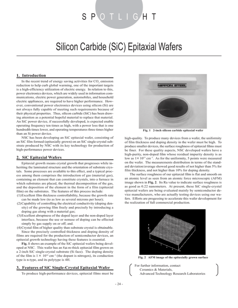
S P O T L I G H T NIPPON STEEL TECHNICAL REPORT No. 92 July 2005 Silicon Carbide (SiC) Epitaxial Wafers 1. Introduction In the recent trend of energy saving activities for CO2 emission reduction to help curb global warming, one of the important targets is a high-efficiency utilization of electric energy. In relation to this, power electronics devices, which are widely used in information communications, electric power generation, automobiles, and household electric appliances, are required to have higher performance. However, conventional power electronics devices using silicon (Si) are not always fully capable of meeting such requirements because of their physical properties. Thus, silicon carbide (SiC) has been drawing attention as a potential hopeful material to replace that material. An SiC power device, if successfully developed, is expected enable operating frequency ten times as high, with a power loss that is one hundredth times lower, and operating temperatures three times higher than an Si power device. NSC has been developing an SiC epitaxial wafer, consisting of an SiC film formed (epitaxially grown) on an SiC single-crystal substrate produced by NSC with its key technology for production of high-performance power devices. Fig. 1 2-inch silicon carbide epitaxial wafer high-quality. To produce many devices from a wafer, the uniformity of film thickness and doping density in the wafer must be high. To produce smaller devices, the surface roughness of epitaxial films must be finer. For these quality aspects, NSC developed wafers have a high-purity, non-doped film whose residual impurity density is as low as 1×1015 cm–3. As for the uniformity, 5 points were measured on the wafer. The measurements distribution in terms of the standard deviation/average showed good results of not higher than 5% for film thickness, and not higher than 10% for doping density. The surface roughness of our epitaxial film is flat and smooth on an atomic level as seen from an atomic force microscopic (AFM) image shown in Fig. 2. Its Ra value to indicate surface roughness is as good as 0.22 nanometers. At present, these SiC single-crystal epitaxial wafers are being evaluated mainly by semiconductor device manufacturers, who are actually testing devices using our wafers. Efforts are progessing to accelerate this wafer development for the realization of full commercial production. 2. SiC Epitaxial Wafers Epitaxial growth means crystal growth that progresses while inheriting the laminated structure and the orientation of substrate crystals. Some processes are available to this effect, and a typical process among them comprises the introduction of gas (material gas), containing an element that can constitute crystals, into a furnace in which substrates are placed, the thermal decomposition of the gas, and the deposition of the element in the form of a film (epitaxial film) on the substrates. The features of this process include: (1)Excellent film thickness controllability, because the growth rate can be made low (to as low as several microns per hour); (2)Capability of controlling the electrical conductivity (doping density) of the growing film freely and precisely by introducing a doping gas along with a material gas; (3)Excellent abruptness of the doped layer and the non-doped layer interface, because the use or nonuse of doping can be effected simply by gas supply on or off; and. (4)Crystal film of higher quality than substrate crystal is obtainable. Since the precisely controlled thickness and doping density of films are required for the production of semiconductor devices, an epitaxial growth technology having these features is essential. Fig. 1 shows an example of the SiC epitaxial wafers being developed at NSC. This wafer has an 8μ m-thick epitaxial film grown on a 2-inch SiC single-crystal substrate (Si face). The doping density of the film is 1 × 1016 cm–3 (the dopant is nitrogen), its conduction type is n-type, and its polytype is 4H. Fig. 2 AFM image of the epitaxially grown surface For further information, contact Ceramics & Materials, Advanced Technology Research Laboratories 3. Features of SiC Single-Crystal Epitaxial Wafer To produce high-performance devices, epitaxial films must be - 24 -


