9. PN Junction Diode
advertisement

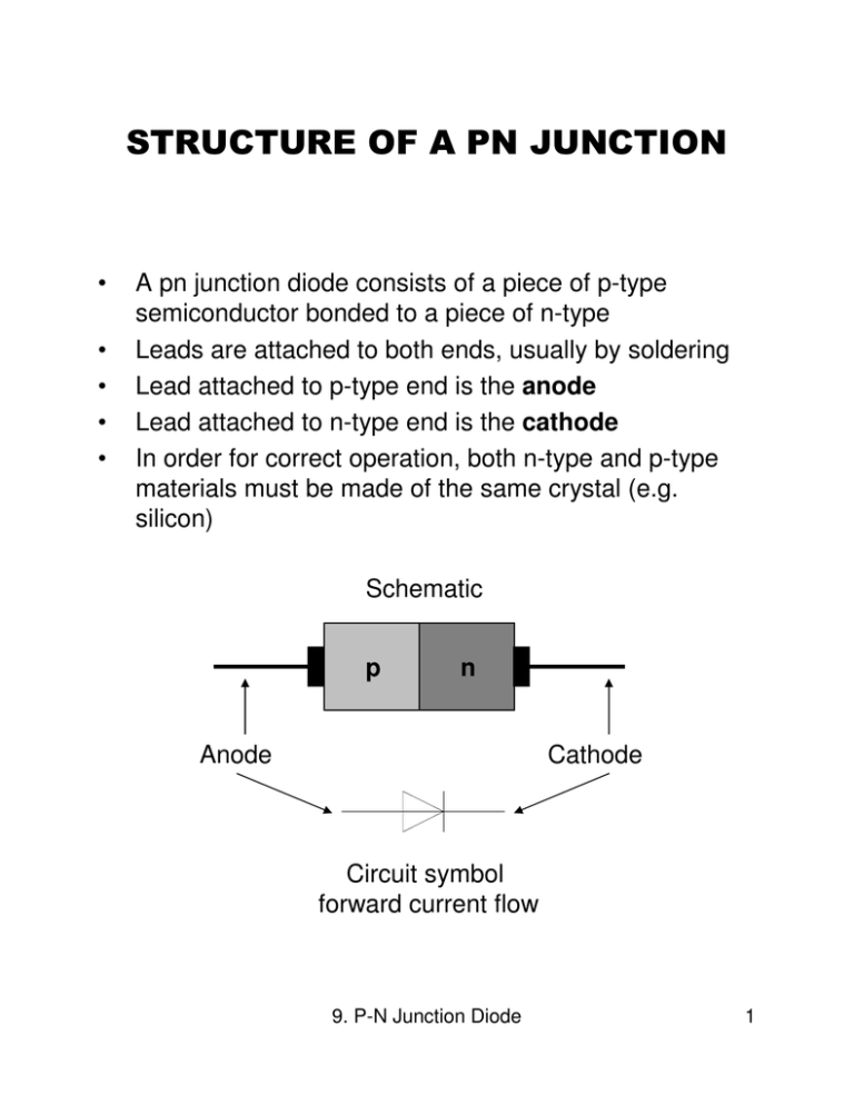
STRUCTURE OF A PN JUNCTION • • • • • A pn junction diode consists of a piece of p-type semiconductor bonded to a piece of n-type Leads are attached to both ends, usually by soldering Lead attached to p-type end is the anode Lead attached to n-type end is the cathode In order for correct operation, both n-type and p-type materials must be made of the same crystal (e.g. silicon) Schematic p n Anode Cathode Circuit symbol forward current flow 9. P-N Junction Diode 1 GENERAL CHARACTERISTICS • • • There are two important characteristics of a pn junction diode Forward bias A large current will flow if voltage is applied in such a direction as to make the p-type material more positive than the n-type Reverse bias A minute current flows if the voltage is reversed in polarity 9. P-N Junction Diode 2 VOLTAGE – CURRENT CHARACTERISTICS • • • When forward biased, current iD flows in the direction from anode (p) to cathode (n) as the voltage across diode (vD) reaches 0.6V When reversed biased, there is no current flow through the diode When a certain reverse biased voltage is reached, breakdown occurs, producing sharp rise in current. May lead to overheating and damage diode. 9. P-N Junction Diode 3 DIODES AS RECTIFIERS • Junction diodes are used in rectifier circuits, such as those in mobile phone chargers, to convert AC into DC • • Above is circuit of half wave rectifier As input increases positively from zero, diode becomes forward biased. Current will flow whenever the instantaneous value of input is greater than about 0.6V When input voltage goes negative, diode becomes reverse biased, and diode behaves like an open circuit when input voltage drops below 0.6V. Output voltage therefore consists of positive half cycles of a sinusoid • • 9. P-N Junction Diode 4 PASSIVE SMOOTHING CIRCUITS • • • • • • For many applications, especially in DC power supplies such as mobile phone rechargers, the output voltage waveform is not smooth enough for acceptable operation Extra components must be added to smoothen the output voltage Passive components do not rely on power supplied from a separate power supply in order to operate Passive smoothing networks consist of combinations of capacitors, inductors and resistors Inductors are rarely used today due to their large size and expense The most commonly used passive technique is the addition of a capacitor connected in parallel with the load 9. P-N Junction Diode 5 CAPACITOR INPUT FILTER AC • • • • • • • Here a rectifier feeds into initially uncharged capacitor During negative half cycle of supply voltage, rectifier is reverse biased, no current flows in circuit During a positive half cycle, rectifier becomes forward biased, allowing current to flow Rectifier thus acts as a short circuit and the voltage across the capacitor follows the supply voltage until it reaches its peak When the supply voltage starts to fall from its positive peak, the capacitor voltage can’t follow it, as it would have to discharge through the diode – which it can’t as no current can flow in the reverse direction – i.e. back through the diode The capacitor will thus remained charged up to the peak of the supply voltage Circuit known as a peak detector 9. P-N Junction Diode 6 CAPACITOR INPUT FILTER AND RESISTIVE LOAD • • • Works similarly to input filter on previous slide However, here as the input voltage falls, the capacitor can now discharge through load resistor RL, which allows the output voltage to fall Rectifier will only conduct when its anode is positive with respect to its cathode which only occurs for a small part of the cycle 9. P-N Junction Diode 7


