Chapter 1-Introduction to Electronics and Design
advertisement
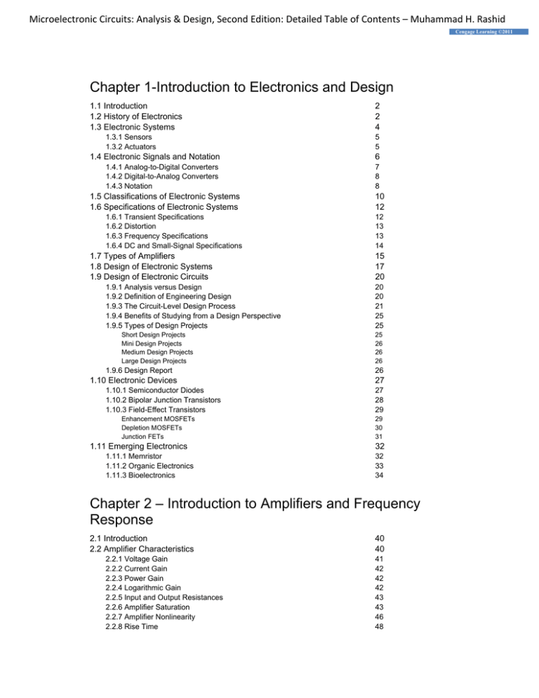
Microelectronic Circuits: Analysis & Design, Second Edition: Detailed Table of Contents – Muhammad H. Rashid Cengage Learning ©2011 Chapter 1-Introduction to Electronics and Design 1.1 Introduction 1.2 History of Electronics 1.3 Electronic Systems 1.3.1 Sensors 1.3.2 Actuators 2 2 4 5 5 1.4 Electronic Signals and Notation 6 1.4.1 Analog-to-Digital Converters 1.4.2 Digital-to-Analog Converters 1.4.3 Notation 7 8 8 1.5 Classifications of Electronic Systems 1.6 Specifications of Electronic Systems 1.6.1 Transient Specifications 1.6.2 Distortion 1.6.3 Frequency Specifications 1.6.4 DC and Small-Signal Specifications 1.7 Types of Amplifiers 1.8 Design of Electronic Systems 1.9 Design of Electronic Circuits 1.9.1 Analysis versus Design 1.9.2 Definition of Engineering Design 1.9.3 The Circuit-Level Design Process 1.9.4 Benefits of Studying from a Design Perspective 1.9.5 Types of Design Projects Short Design Projects Mini Design Projects Medium Design Projects Large Design Projects 1.9.6 Design Report 1.10 Electronic Devices 1.10.1 Semiconductor Diodes 1.10.2 Bipolar Junction Transistors 1.10.3 Field-Effect Transistors Enhancement MOSFETs Depletion MOSFETs Junction FETs 1.11 Emerging Electronics 1.11.1 Memristor 1.11.2 Organic Electronics 1.11.3 Bioelectronics 10 12 12 13 13 14 15 17 20 20 20 21 25 25 25 26 26 26 26 27 27 28 29 29 30 31 32 32 33 34 Chapter 2 – Introduction to Amplifiers and Frequency Response 2.1 Introduction 2.2 Amplifier Characteristics 2.2.1 Voltage Gain 2.2.2 Current Gain 2.2.3 Power Gain 2.2.4 Logarithmic Gain 2.2.5 Input and Output Resistances 2.2.6 Amplifier Saturation 2.2.7 Amplifier Nonlinearity 2.2.8 Rise Time 40 40 41 42 42 42 43 43 46 48 Microelectronic Circuits: Analysis & Design, Second Edition: Detailed Table of Contents – Muhammad H. Rashid Cengage Learning ©2011 2.2.9 Slew Rate 2.3 Amplifier Types 2.3.1 Voltage Amplifiers 2.3.2 Current Amplifiers 2.3.3 Transconductance Amplifiers 2.3.4 Transimpedance Amplifiers 2.4 Cascaded Amplifiers 2.4.1 Cascaded Voltage Amplifiers 2.4.2 Cascaded Current Amplifiers 2.5 Frequency Response of Amplifiers 2.5.1 Low-Pass Characteristic 2.5.2 High-Pass Characteristic 2.5.3 Band-Pass Characteristic 2.5.4 Gain and Bandwidth Relation 2.6 Miller’s Theorem 2.7 Frequency Response Methods 2.7.1 Low-Frequency Transfer Function Method 2.7.2 High-Frequency Transfer Function Method 2.7.3 Miller’s Capacitor Method 2.7.4 Low-Frequency Short-Circuit Method 2.7.5 High-Frequency Zero-Value Method 2.7.6 Midband Voltage Gain 2.7.7 Multistage Amplifiers 2.8 PSpice/SPICE Amplifier Models 2.8.1 Voltage Amplifier 2.8.2 Current Amplifier 2.8.3 Transconductance Amplifier 2.8.4 Transimpedance Amplifier 2.9 Amplifier Design 48 50 51 53 55 57 59 59 60 62 63 66 68 69 71 72 73 75 77 80 82 84 86 87 87 87 88 88 88 Chapter 3 – Introduction to Operational Amplifiers and Applications 3.1 Introduction 3.2 Characteristics of Ideal Op-Amps 3.2.1 Op-Amp Circuit Model 3.2.2 Op-Amp Frequency Response 3.2.3 Common-Mode Rejection Ratio 3.3 Op-Amp PSpice/SPICE Models 3.3.1 DC Linear Model 3.3.2 AC Linear Model 3.3.3 Nonlinear Macromodel 3.4 Analysis of Ideal Op-Amp Circuits 3.4.1 Noninverting Amplifiers CMRR of a Noninverting Amplifier 3.4.2 Inverting Amplifiers CMRR of an Inverting Amplifier 3.5 Op-Amp Applications 3.5.1 Integrators Frequency Response of Op-Amp Integrators 3.5.2 Differentiators Frequency Response of Op-Amp Differentiators 3.5.3 Differential Amplifiers CMRR of a Differential Amplifier 3.5.4 Instrumentation Amplifiers CMRR of an Instrumentation Amplifier 3.5.5 Noninverting Summing Amplifiers 104 104 105 107 108 111 111 112 113 114 114 116 121 122 128 128 134 137 141 143 144 145 146 147 Microelectronic Circuits: Analysis & Design, Second Edition: Detailed Table of Contents – Muhammad H. Rashid Cengage Learning ©2011 3.5.6 Inverting Summing Amplifiers 3.5.7 Addition–Subtraction Amplifiers 3.5.8 Optocoupler Drivers 3.5.9 Photodetectors 3.5.10 Voltage–Current Converters 3.5.11 DC Voltmeters 3.5.12 DC Millivoltmeters 3.5.13 Negative Impedance Converters 3.5.14 Constant Current Sources 3.5.15 Noninverting Integrators 3.5.16 Inductance Simulators 3.5.17 AC-Coupled Bootstrapped Voltage Followers 3.6 Op-Amp Circuit Design 148 149 153 154 155 156 157 158 159 159 161 162 164 Chapter 4 – Semiconductor Diodes 4.1 Introduction 4.2 Ideal Diodes 4.3 Transfer Characteristics of Diode Circuits 4.4 Practical Diodes 4.4.1 Characteristic of Practical Diodes Forward-Biased Region Reverse-Biased Region Breakdown Region 4.4.2 Determination of Diode Constants 4.4.3 Temperature Effects 4.5 Analysis of Practical Diode Circuits 180 180 183 185 185 186 186 187 187 189 192 4.5.1 Graphical Method 4.5.2 Approximate Method 4.5.3 Iterative Method 4.5.4 Mathematical Method 192 193 193 194 4.6 Modeling of Practical Diodes 196 4.6.1 Constant-Drop DC Model 4.6.2 Piecewise Linear DC Model 4.6.3 Low-Frequency Small-Signal Model Determining rd by Differentiating Determining rd by Taylor Series Expansion 4.6.4 PSpice/SPICE Diode Model Model Statement Tabular Representation 4.7 Zener Diodes 4.7.1 Zener Regulator 4.7.2 Design of a Zener Regulator 4.7.3 Zener Limiters 4.7.4 Temperature Effects on Zener Diodes 4.8 Light-Emitting Diodes 4.9 Power Rating 4.10 Diode Data Sheets 196 197 199 201 201 205 205 206 208 209 211 214 218 220 220 222 Chapter 5 – Applications of Diodes 5.1 Introduction 5.2 Diode Rectifier 5.2.1 Single-Phase Half-Wave Rectifiers 5.2.2 Single-Phase Full-Wave Center-Tapped Rectifier 5.2.3 Single-Phase Full-Wave Bridge Rectifier 238 238 238 247 254 Microelectronic Circuits: Analysis & Design, Second Edition: Detailed Table of Contents – Muhammad H. Rashid Cengage Learning ©2011 5.3 Output Filters for Rectifiers 5.3.1 L Filters 5.3.2 C Filters 5.3.3 LC Filters 5.4 Diode Peak Detectors and Demodulators 5.5 Diode Clippers 5.5.1 Parallel Clippers 5.5.2 Series Clippers 5.6 Diode Clamping Circuits 5.6.1 Fixed-Shift Clampers 5.6.2 Variable-Shift Clampers 5.7 Diode Voltage Multipliers 5.7.1 Voltage Doublers 5.7.2 Voltage Triplers and Quadruplers 5.8 Diode Function Generators 260 261 264 269 272 276 277 278 280 280 281 285 285 287 290 Chapter 6 – Semiconductors and pn Junction Characteristics 6.1 Introduction 6.2 Semiconductor Materials 6.2.1 n-type Materials 6.2.2 p-type Materials 6.2.3 Majority and Minority Carriers 6.2.4 The Fermi Function 6.2.5 Carrier Concentrations 6.3 Zero-Biased pn Junction 6.3.1 Built-In Junction Potential 6.3.2 Electric Field Distribution 6.3.3 Junction Potential Distribution 6.3.4 Space Charge Depletion Width 6.4 Reverse-Biased pn Junction 6.4.1 Breakdown Condition 6.4.2 Depletion Region Width 6.4.3 Junction Capacitance 6.5 Forward-Biased pn Junction 6.5.1 Depletion Region Width 6.5.2 Minority Carrier Charge Distribution 300 300 301 302 303 304 305 307 308 310 311 312 314 315 316 317 319 320 321 6.6 Junction Current Density 6.7 Temperature Dependence 6.8 High-Frequency AC Model 323 325 326 6.8.1 Depletion Capacitance 6.8.2 Diffusion Capacitance 6.8.3 Forward-Biased Model 6.8.4 Reverse-Biased Model 326 327 328 329 Chapter 7 – Metal Oxide Semiconductor Field-Effect Transistors 7.1 Introduction 7.2 Metal Oxide Field-Effect Transistors 7.3 Enhancement MOSFETs 7.3.1 Operation Cutoff Region 336 336 337 338 338 Microelectronic Circuits: Analysis & Design, Second Edition: Detailed Table of Contents – Muhammad H. Rashid Cengage Learning ©2011 Linear Ohmic Region Nonlinear Ohmic Region Saturation Region 7.3.2 Output and Transfer Characteristics 7.3.3 Channel Length Modulation 7.3.4 Substrate Biasing Effects 7.3.5 Complementary MOS (CMOS) 7.4 Depletion MOSFETs 7.4.1 Operation 7.4.2 Output and Transfer Characteristics Ohmic Region Saturation Region Cutoff Region 339 340 341 342 343 345 346 346 347 349 349 349 349 7.5 MOSFET Models and Amplifier 349 7.5.1 DC Models 7.5.2 Small-Signal AC Models 351 351 Small-Signal Output Resistance ro Transconductance gm 352 352 7.5.3 PSpice Models 7.5.4 Small-Signal Analysis 353 354 7.6 A MOSFET Switch 7.7 DC Biasing of MOSFETs 356 357 7.7.1 MOSFET Biasing Circuit 7.7.2 Design of MOSFET Biasing Circuit 7.8 Common-Source (CS) Amplifiers 7.8.1 CS Amplifier with Current Source Load 7.8.2 CS Amplifier with Enhancement MOSFET Load 7.8.3 CS Amplifier with Depletion MOSFET Load 7.8.4 CS Amplifier with Resistive Load Input Resistance Ri () Output Resistance Ro Open-Circuit (or No-Load) Voltage Gain Avo 7.9 Common-Drain Amplifiers 7.9.1 Active-Biased Source Follower Input Resistance Ri Voltage Gain Avo Output Resistance Ro 7.9.2 Resistive-Biased Source Follower Input Resistance Ri Output Resistance Ro 7.10 Common-Gate Amplifiers Input Resistance Ri No-Load Voltage Gain Avo Output Resistance Ro 7.11 Multistage Amplifiers 7.11.1 Capacitor-Coupled Cascaded Amplifiers 7.11.2 Direct-Coupled Amplifiers 7.11.3 Cascoded Amplifiers DC Biasing Small-Signal Voltage Gain Small-Signal Output Resistance 7.12 DC Level Shifting and Amplifier 7.12.1 Level-Shifting Methods Potential Divider Level Shifting Current Source Level Shifting Zener Level Shifting 7.12.2 Level-Shifted MOS Amplifier Current Mirror Source Small-Signal Voltage Gain 7.13 Frequency Response of MOSFET Amplifiers 359 359 365 365 368 370 371 372 372 374 375 376 376 376 376 378 378 379 380 380 382 382 383 383 383 384 384 386 386 386 387 387 387 388 388 388 390 393 Microelectronic Circuits: Analysis & Design, Second Edition: Detailed Table of Contents – Muhammad H. Rashid Cengage Learning ©2011 7.13.1 High-Frequency MOSFET Models 7.13.2 Small-Signal PSpice Model 7.13.3 Common-Source Amplifiers Low Cutoff Frequencies High Cutoff Frequencies 7.13.4 Common-Drain Amplifiers Low Cutoff Frequencies High Cutoff Frequencies 7.13.5 Common-Gate Amplifiers Low Cutoff Frequencies High Cutoff Frequencies 7.14 Design of MOSFET Amplifiers 393 395 396 397 398 401 401 402 403 403 404 408 Chapter 8 – Bipolar Junction Transistors and Amplifiers 8.1 Introduction 8.2 Bipolar Junction Transistors 8.3 Principles of BJT Operation 8.3.1 Forward Mode of Operation Collector Current Emitter Current Base Current Forward-Current Ratio Forward-Current Gain 8.3.2 Cutoff, Saturation, and Inverse-Active Modes of Operation 8.3.3 Base Narrowing 8.3.4 Physical Parameters of Saturation Current IS and Current Gain Collector Saturation Current ISC Base Saturation Current ISB Current Gain bF 8.4 Input and Output Characteristics 8.5 BJT Circuit Models 8.5.1 Linear DC Model 8.5.2 Small-Signal AC Model 8.5.3 Small-Signal Hybrid Model 8.5.4 PSpice/SPICE Model 8.5.5 Small-Signal Analysis 8.6 The BJT Switch 8.7 dc Biasing of Bipolar Junction Transistors 8.7.1 Active Current–Source Biasing 8.7.2 Single–Base Resistor Biasing 8.7.3 Emitter Resistance–Feedback Biasing 8.7.4 Emitter-Follower Biasing 8.7.5 Two–Base Resistor Biasing 8.7.6 Biasing Circuit Design 8.8 Common-Emitter Amplifiers 434 434 436 436 439 439 440 440 440 440 441 444 445 445 446 447 449 450 450 452 452 453 455 457 458 459 460 461 461 463 467 8.8.1 Active-Biased Common-Emitter Amplifier 8.8.2 Resistive-Biased Common-Emitter Amplifier 468 471 Input Resistance Ri Output Resistance Ro Open-Circuit (or No-Load) Voltage Gain Avo 472 473 473 8.9 Emitter Followers 8.9.1 Active-Biased Emitter Follower Input Resistance Ri Open-Circuit (or No-Load) Voltage Gain Avo Output Resistance Ro 8.9.2 Resistive-Biased Emitter Follower 8.10 Common-Base Amplifiers 8.10.1 Input Resistance Ri 476 476 476 477 478 479 483 484 Microelectronic Circuits: Analysis & Design, Second Edition: Detailed Table of Contents – Muhammad H. Rashid Cengage Learning ©2011 8.10.2 No-Load Voltage Gain Avo 8.10.3 Output Resistance Ro 8.11 Multistage Amplifiers 8.11.1 Capacitor-Coupled Cascaded Amplifiers 8.11.2 Direct-Coupled Amplifiers 8.11.3 Cascoded Amplifiers DC Biasing Small-Signal Voltage Gain Small-Signal Output Resistance 8.12 The Darlington Pair Transistor 8.13 DC Level Shifting and Amplifier 8.13.1 Level-Shifting Methods Potential Divider Level Shifting Current Source Level Shifting Zener Level Shifting 485 485 488 488 489 489 489 489 491 491 495 496 496 497 497 8.13.2 Level-Shifted dc Amplifier 497 Current Mirror Source DC Output Voltage Small-Signal Voltage Gain 497 499 500 8.14 Frequency Model and Response of Bipolar Junction Transistors 501 8.14.1 High-Frequency Model 8.14.2 Small-Signal PSpice/SPICE Model 8.14.3 Frequency Response of BJTs 501 503 504 8.15 Frequency Response of BJT Amplifiers 508 8.15.1 Common-Emitter BJT Amplifiers Low Cutoff Frequencies High Cutoff Frequencies 8.15.2 Common-Collector BJT Amplifiers Low Cutoff Frequencies High Cutoff Frequencies 8.15.3 Common-Base BJT Amplifiers Low Cutoff Frequencies High Cutoff Frequencies 508 508 510 514 515 516 518 518 520 8.15.4 Multistage Amplifiers 522 8.16 MOSFETs versus BJTs 8.17 Design of Amplifiers 528 528 8.17.1 BJT Amplifier Design Designing for Specified Voltage Gain Designing for Specified Input Resistance 529 530 532 Chapter 9 – Differential Amplifiers 9.1 Introduction 9.2 Internal Structure of Differential Amplifiers 9.2.1 Characteristics of Differential Amplifiers 9.2.2 Internal Structure of Differential Amplifiers 9.3 MOSFET Current Sources 9.3.1 Basic Current Source 9.3.2 Modified Basic Current Source Output Resistance Ro 9.3.3 Multiple Current Sources Output Resistance Ro 9.3.4 Cascode Current Source 9.3.5 Wilson Current Source 9.3.6 Design of Active Current Sources 9.4 MOS Differential Amplifiers 9.4.1 NMOS Differential Pair dc Transfer Characteristics Small-Signal Analysis 554 554 554 557 558 559 561 561 563 563 563 564 565 566 566 567 569 Microelectronic Circuits: Analysis & Design, Second Edition: Detailed Table of Contents – Muhammad H. Rashid Cengage Learning ©2011 9.4.2 MOS Differential Pair with Active Load 9.4.3 Cascoded MOS Differential Amplifier 9.5 Depletion MOS Differential Amplifiers 9.5.1 Depletion MOS Differential Pair with Resistive Load dc Transfer Characteristics Small-Signal Analysis 9.5.2 Depletion MOS Differential Pair with Active Load 9.6 BJT Current Sources 9.6.1 Basic Current Source Output Resistance Ro 9.6.2 Modified Basic Current Source 575 578 580 581 581 583 585 586 586 587 589 Output Resistance Ro 590 9.6.3 Widlar Current Source 591 Output Resistance Ro 9.6.4 Cascode Current Source 9.6.5 Wilson Current Source Output Resistance Ro 9.6.6 Multiple Current Sources 9.7 BJT Differential Amplifiers 9.7.1 BJT Differential Pair with Resistive Load dc Transfer Characteristics Small-Signal Analysis 9.7.2 BJT Differential Amplifiers with Basic Current Mirror Active Load Small-Signal Analysis 9.7.3 Differential Amplifier with Modified Current Mirror 9.7.4 Cascode Differential Amplifier 9.8 BiCMOS Differential Amplifiers 9.8.1 BJT versus CMOS Amplifiers 9.8.2 BiCMOS Amplifiers 9.8.3 Cascode BiCMOS Amplifiers 9.8.4 Double-Cascode BiCMOS Amplifiers 593 595 596 598 601 602 602 603 606 613 614 615 617 620 620 621 622 623 9.9 Frequency Response of Differential Amplifiers 626 9.9.1 Frequency Response with Resistive Load 9.9.2 Frequency Response with Active Load 626 627 9.10 Design of Differential Amplifiers 628 Chapter 10 – Feedback Amplifiers 10.1 Introduction 10.2 Feedback 10.3 Characteristics of Feedback 10.3.1 Closed-Loop Gain 10.3.2 Gain Sensitivity 10.3.3 Feedback Factor Sensitivity 10.3.4 Frequency Response 10.3.5 Distortion 10.4 Feedback Topologies 642 643 644 644 646 646 648 649 652 10.4.1 Feedback Configurations 10.4.2 Feedback Relationships 652 655 10.5 Analysis of Feedback Amplifiers 10.6 Series-Shunt Feedback 656 657 10.6.1 Analysis of an Ideal Series-Shunt Feedback Network 10.6.2 Analysis of a Practical Series-Shunt Feedback Network 10.7 Series-Series Feedback 10.7.1 Analysis of an Ideal Series-Series Feedback Network 10.7.2 Analysis of a Practical Series-Series Feedback Network 10.8 Shunt-Shunt Feedback 658 661 667 669 670 677 Microelectronic Circuits: Analysis & Design, Second Edition: Detailed Table of Contents – Muhammad H. Rashid Cengage Learning ©2011 10.8.1 Analysis of an Ideal Shunt-Shunt Feedback Network 10.8.2 Analysis of a Practical Shunt-Shunt Feedback Network 10.9 Shunt-Series Feedback 10.9.1 Analysis of an Ideal Shunt-Series Feedback Network 10.9.2 Analysis of a Practical Shunt-Series Feedback Network 10.10 Feedback Circuit Design 10.11 Stability Analysis 10.11.1 Closed-Loop Frequency and Stability 10.11.2 Poles and Instability 10.11.3 Transient Response and Stability 10.11.4 Closed-Loop Poles and Stability 10.11.5 Nyquist Stability Criterion 10.11.6 Relative Stability 10.11.7 Effects of Phase Margin 10.11.8 Stability Using Bode Plots 10.12 Compensation Techniques 10.12.1 Addition of a Dominant Pole 10.12.2 Changing the Dominant Pole 10.12.3 Miller Compensation and Pole Splitting 10.12.4 Modification of the Feedback Path 678 680 686 688 688 692 698 698 699 699 700 703 704 705 707 711 711 713 715 717 Chapter 11 – Power Amplifiers 11.1 Introduction 11.2 Classification of Power Amplifiers 11.3 Power Transistors 11.4 Class A Amplifiers 11.4.1 Emitter Followers Transfer Characteristic Signal Waveforms Output Power and Efficiency 11.4.2 Basic Common-Emitter Amplifier Transfer Characteristic Output Power and Efficiency 11.4.3 Common-Emitter Amplifiers with Active Load Transfer Characteristic Output Power and Efficiency 11.4.4 Transformer-Coupled Load Common-Emitter Amplifier 11.5 Class B Push-Pull Amplifiers 11.5.1 Complementary Push-Pull Amplifiers Output Power and Efficiency Dead-Zone Minimization 11.5.2 Transformer-Coupled Load Push-Pull Amplifier Signal Waveforms Output Power and Efficiency dc Biasing 11.6 Complementary Class AB Push-Pull Amplifiers 11.6.1 Transfer Characteristic 11.6.2 Output Power and Efficiency 11.6.3 Biasing with Diodes 11.6.4 Biasing with Diodes and an Active Current Source Transfer Characteristic 11.6.5 Biasing with a VBE Multiplier 11.6.6 Quasi-Complementary Class AB Amplifiers 11.6.7 Transformer-Coupled Class AB Amplifiers 11.7 Class C Amplifiers 11.8 Class D Amplifiers 11.10 Short-Circuit and Thermal Protection 740 740 743 745 745 746 746 746 749 749 750 752 752 753 753 756 756 757 759 761 761 762 764 766 767 767 767 769 770 772 775 776 777 784 786 Microelectronic Circuits: Analysis & Design, Second Edition: Detailed Table of Contents – Muhammad H. Rashid Cengage Learning ©2011 11.10.1 Short-Circuit Protection 11.10.2 Thermal Protection 786 787 11.11 Power Op-Amps 11.11.1 IC Power Amplifiers 788 789 Power Op-Amp LH0021 Power Op-Amp LM380 789 790 11.11.2 Bridge Amplifier 791 11.12 Thermal Considerations 792 11.12.1 Thermal Resistance 11.12.2 Heat Sink and Heat Flow 11.12.3 Power Dissipation versus Temperature 11.13 Design of Power Amplifiers 793 793 794 796 Chapter 12 – Active Filters 12.1 Introduction 12.2 Active versus Passive Filters 12.3 Types of Active Filters 12.4 First-Order Filters 12.5 The Biquadratic Function 12.6 Butterworth Filters 12.6.1 Butterworth Function for n 5 1 12.6.2 Butterworth Function for n 5 2 12.6.3 Butterworth Function for n 5 3 12.6.4 Butterworth Function for Higher-Order Filters 12.7 Transfer Function Realization 12.8 Low-Pass Filters 12.8.1 First-Order Low-Pass Filters 12.8.2 Second-Order Low-Pass Filters 12.8.3 Butterworth Low-Pass Filters 12.9 High-Pass Filters 12.9.1 First-Order High-Pass Filters 12.9.2 Second-Order High-Pass Filters 12.9.3 Butterworth High-Pass Filters 12.10 Band-Pass Filters 12.10.1 Wide-Band-Pass Filters 12.10.2 Narrow-Band-Pass Filters 12.11 Band-Reject Filters 12.11.1 Wide-Band-Reject Filters 12.11.2 Narrow-Band-Reject Filters 12.12 All-Pass Filters 12.13 Switched-Capacitor Filters 12.13.1 Switched-Capacitor Resistors 12.13.2 Switched-Capacitor Integrators 12.13.3 Universal Switched-Capacitor Filters 12.14 Filter Design Guidelines 804 804 805 808 810 814 815 815 816 816 818 819 819 822 826 829 829 831 834 837 837 840 843 844 846 848 849 850 851 851 854 Chapter 13 - Oscillators 13.1 Introduction 13.2 Principles of Oscillators 862 862 13.2.1 Conditions for Oscillations 13.2.2 Frequency Stability 13.2.3 Amplitude Stability 863 866 866 13.3 Audio-Frequency Oscillators 867 Microelectronic Circuits: Analysis & Design, Second Edition: Detailed Table of Contents – Muhammad H. Rashid Cengage Learning ©2011 13.3.1 Phase-Shift Oscillators 13.3.2 Quadrature Oscillators 13.3.3 Three-Phase Oscillators 13.3.4 Wien-Bridge Oscillators 13.3.5 Ring Oscillators 13.4 Radio Frequency Oscillators 867 871 873 874 878 881 13.4.1 Colpitts Oscillators 13.4.2 Hartley Oscillators 13.4.3 Two-Stage MOS Oscillators 881 888 891 13.5 Crystal Oscillators 13.6 Active-Filter Tuned Oscillators 13.7 Design of Oscillators 895 899 902 Chapter 14 – Operational Amplifiers 14.1 Introduction 14.2 Internal Structure of Op-Amps 14.3 Parameters and Characteristics of Practical Op-Amps 14.3.1 Input Biasing Current 14.3.2 Input Offset Current 14.3.3 Input Offset Voltage 14.3.4 Power Supply Rejection Ratio 14.3.5 Thermal Voltage Drift 14.3.6 Determining the Thermal Voltage Drift BJT Amplifiers CMOS Amplifiers 910 910 911 912 914 917 918 919 920 921 921 14.3.7 Offset Voltage Adjustment 14.3.8 Common-Mode Rejection Ratio 14.3.9 Input Resistance 14.3.10 Output Resistance 14.3.11 Frequency Response 922 925 925 927 927 Effects of Cx on Unity-Gain Bandwidth Effects of Cx on Zeros 928 929 14.3.12 Slew Rate Relation between SR and fu 14.4 CMOS Op-Amps 14.4.1 Basic CMOS Op-Amp 14.4.2 CMOS Op-Amp MC14573 Differential Stage Gain Stage DC Biasing 14.4.3 CMOS Op-Amp TLC1078 Differential Stage Gain Stage Output Stage DC Biasing 14.5 BJT Op-Amps 14.5.1 BJT Op-Amp LM124 Differential Stage Gain Stage Output Stage 930 931 933 933 934 935 935 935 937 938 938 938 939 940 940 940 941 942 14.5.2 BJT Op-Amp LM741 942 Differential Stage Gain Stage Output Stage Protection Circuitry 942 944 944 944 14.6 Analysis of the LM741 Op-Amp 14.6.1 DC Analysis Biasing Circuit 944 944 945 Microelectronic Circuits: Analysis & Design, Second Edition: Detailed Table of Contents – Muhammad H. Rashid Cengage Learning ©2011 Input Stage Gain Stage Output Stage Overload Protection 14.6.2 Small-Signal AC Analysis Input Stage Gain Stage Output Stage 14.6.3 Frequency-Response Analysis 14.6.4 Small-Signal Equivalent Circuit 14.7 BiCMOS Op-Amps 14.7.1 BiCMOS Op-Amp CA3130 Differential Stage Gain Stage Output Stage 14.7.2 BiCMOS Op-Amp CA3140 Output Stage 14.7.3 BiCMOS Op-Amp LH0022 Differential Stage Gain Stage Output Stage Protection Circuitry Biasing Circuitry 14.7.4 BiCMOS Op-Amp LF411 DC Biasing Thermal Protection 14.7.5 BiCMOS Op-Amp LH0062 Differential Stage Gain Stage 14.7.6 BiCMOS Op-Amp LH0032 14.8 Design of Op-Amps 946 948 949 951 951 952 957 958 961 961 962 962 963 964 964 964 965 965 965 967 967 967 967 969 970 971 971 971 972 973 974 Chapter 15 – Introduction to Digital Electronics 15.1 Introduction 15.2 Logic States 15.3 Logic Gates 15.4 Performance Parameters of Logic Gates 15.4.1 Voltage Transfer Characteristic 15.4.2 Noise Margins 15.4.3 Fan-Out and Fan-In 15.4.4 Propagation Delay 15.4.5 Power Dissipation Static Power Dynamic Power 15.4.6 Delay-Power Product 15.5 NMOS Inverters 15.5.1 NMOS Inverter with Enhancement Load Enhancement Load Static Characteristics Body Effect 15.5.2 NMOS Inverter with Depletion Load Static Characteristics Body Effect 15.5.3 Comparison of NMOS Inverters 15.6 NMOS Logic Circuits 15.6.1 NMOS Transmission Gates 15.6.2 NMOS NOR Gates 15.6.3 NMOS NAND Gates 982 982 983 985 986 987 988 991 992 993 993 995 996 996 996 997 1001 1005 1005 1008 1013 1014 1014 1015 1016 Microelectronic Circuits: Analysis & Design, Second Edition: Detailed Table of Contents – Muhammad H. Rashid Cengage Learning ©2011 15.7 CMOS Inverters 15.8 CMOS Logic Circuits 15.8.1 CMOS Transmission Gates Propagation Delay 15.8.2 CMOS NOR and NAND Gates 15.8.3 CMOS Families 1016 1022 1022 1023 1024 1025 15.9 Comparison of CMOS and NMOS Gates 15.10 BJT Inverters 1026 1026 15.10.1 Voltage Transfer Characteristics 15.10.2 Switching Characteristics 1027 1028 15.11 Transistor-Transistor Logic Gates 15.11.1 Standard TTL Gates 15.11.2 High-Speed TTL NAND Gates 15.11.3 Schottky TTL NAND Gates 15.12 Emitter-Coupled Logic OR/NOR Gates 15.13 BiCMOS Inverters 1033 1034 1042 1047 1049 1057 15.13.1 Propagation Delay 1058 15.14 Interfacing of Logic Gates 1060 15.14.1 TTL Driving CMOS 1060 Current Sinking Current Sourcing 15.14.2 CMOS Driving TTL Current Sourcing Current Sinking 15.15 Comparison of Logic Gates 15.16 Design of Logic Circuits 1061 1061 1062 1062 1063 1063 1064 Chapter 16 – Integrated Analog Circuits and Applications 16.1 Introduction 16.2 Circuits with Op-Amps and Diodes 16.2.1 Most Positive Signal Detectors 16.2.2 Precision Peak Voltage Detectors 16.2.3 Precision Half-Wave Rectifiers 16.2.4 Precision Full-Wave Rectifiers 16.2.5 Precision Clamping Circuits 16.2.6 Fixed-Voltage Limiters 16.2.7 Adjustable Voltage Limiters 16.2.8 Zener Voltage Limiters 16.2.9 Hard Limiters 16.3 Comparators 16.3.1 Comparators versus Op-Amps 16.3.2 Output-Side Connection 16.3.3 Threshold Comparators 16.4 Zero-Crossing Detectors 16.5 Schmitt Triggers 16.5.1 Inverting Schmitt Trigger Transfer Characteristics Effect of Positive Feedback 16.5.2 Noninverting Schmitt Trigger Transfer Characteristics 16.5.3 Schmitt Trigger with Reference Voltage 16.5.4 Effects of Hysteresis on the Output Voltage 16.6 Square-Wave Generators 16.7 Triangular-Wave Generators 16.8 Sawtooth-Wave Generators 16.9 Voltage-Controlled Oscillators 1080 1080 1081 1081 1082 1084 1085 1086 1086 1093 1094 1097 1098 1098 1098 1100 1101 1102 1103 1103 1105 1106 1106 1107 1110 1113 1117 1120 Microelectronic Circuits: Analysis & Design, Second Edition: Detailed Table of Contents – Muhammad H. Rashid Cengage Learning ©2011 16.9.1 Charging Mode 16.9.2 Discharging Mode 16.9.3 Circuit Implementation Voltage-Controlled Current Source Current Switch 16.9.4 The NE/SE-566 VCO 16.10 The 555 Timer 16.10.1 Functional Block Diagram 16.10.2 Monostable Multivibrators 16.10.3 Applications of Monostable Multivibrators Frequency Divider Missing-Pulse Detector Pulse Widener 16.10.4 Astable Multivibrators 16.10.5 Applications of Astable Multivibrators Square-Wave Generator Ramp Generator FSK Modulator 16.11 Phase-Lock Loops 16.11.1 Phase Detector 16.11.2 Integrated Circuit PLL 16.11.3 Applications of the 565 PLL Frequency Multiplier FSK Demodulator SCA (Background Music) Decoder 16.12 Voltage-to-Frequency and Frequency-to-Voltage Converters 16.12.1 V/F Converter 16.12.2 F/V Converter 16.13 Sample-and-Hold Circuits 16.13.1 SAH Op-Amp Circuits 16.13.2 SAH Integrated Circuits 16.14 Digital-to-Analog Converters 16.14.1 Weighted-Resistor D/A Converter 16.14.2 R-2R Ladder Network D/A Converter 16.14.3 Integrated Circuit D/A Converters 16.15 Analog-to-Digital Converters 1120 1121 1121 1121 1122 1123 1126 1126 1127 1129 1129 1129 1130 1131 1134 1134 1135 1137 1139 1140 1141 1143 1143 1145 1145 1147 1147 1151 1155 1157 1157 1158 1159 1160 1162 1165 16.15.1 Successive-Approximation A/D Converter 16.15.2 Integrated Circuit A/D Converters 1165 1167 16.16 Circuit Design Using Analog Integrated Circuits 1169 Appendix A – Introduction to OrCAD A.1 Introduction A.2 Installing the Software A.3 Overview A.4 The Circuit Analysis Process A.5 Drawing the Circuit A.5.1 Beginning a New Project A.5.2 Getting and Placing Components A.5.3 Rotating Components A.5.4 Wiring Components A.5.5 Labeling Components and Adding Text A.5.6 Setting Attributes A.5.7 Viewing the Schematic A.5.8 Saving the Circuit File A.6 Selecting the Type of Analysis A.7 Simulation with PSpice 1178 1178 1180 1181 1182 1182 1183 1185 1187 1187 1188 1190 1190 1191 1193 Microelectronic Circuits: Analysis & Design, Second Edition: Detailed Table of Contents – Muhammad H. Rashid Cengage Learning ©2011 A.8 Displaying the Results of a Simulation A.9 Copying and Capturing Schematics A.10 Varying Parameters A.11 Frequency Response Analysis A.12 Modeling Devices and Elements A.12.1 Resistors A.12.2 Capacitors A.12.3 Inductors A.12.4 Diodes A.12.5 Bipolar Transistors A.12.6 JFETs A.12.7 MOSFETs A.13 Creating Netlists A.14 Adding Library Files 1194 1196 1196 1198 1200 1201 1202 1202 1203 1203 1204 1204 1206 1208 Appendix B - Review of Basic Circuits B.1 Introduction B.2 Kirchhoff’s Current Law B.3 Kirchhoff’s Voltage Law B.4 Superposition Theorem B.5 Thevenin’s Theorem B.6 Norton’s Theorem B.7 Maximum Power Transfer Theorem B.8 Transient Response of First-Order Circuits B.8.1 Step Response of Series RC Circuits B.8.2 Step Response of Series CR Circuits B.8.3 Pulse Response of Series RC Circuits B.8.4 Pulse Response of Series CR Circuits B.8.5 Step Response of Series RL Circuits B.9 Resonant Circuits B.9.1 Series Resonant Circuits B.9.2 Parallel Resonant Circuits B.10 Frequency Response of First- and Second-Order Circuits B.10.1 First-Order Low-Pass RC Circuits B.10.2 First-Order High-Pass CR Circuits B.10.3 Second-Order Series RLC Circuits B.10.4 Second-Order Parallel RLC Circuits B.11 Time Constants of First-Order Circuits 1214 1214 1216 1219 1221 1226 1227 1228 1229 1230 1231 1234 1237 1238 1239 1240 1243 1244 1246 1249 1254 1258 Appendix C - Low-Frequency Hybrid BJT Model Appendix D - Ebers–Moll Model of Bipolar Junction Transistors Appendix E - Passive Components E.1 Resistors E.2 Potentiometers E.3 Capacitors 1276 1278 1279 Microelectronic Circuits: Analysis & Design, Second Edition: Detailed Table of Contents – Muhammad H. Rashid Cengage Learning ©2011 Appendix F - Design Problems Mini Design Projects Medium Design Projects Large Design Projects 1282 1282 1282
