5W X-Band GaN Power Amplifier Using a Commercially
advertisement

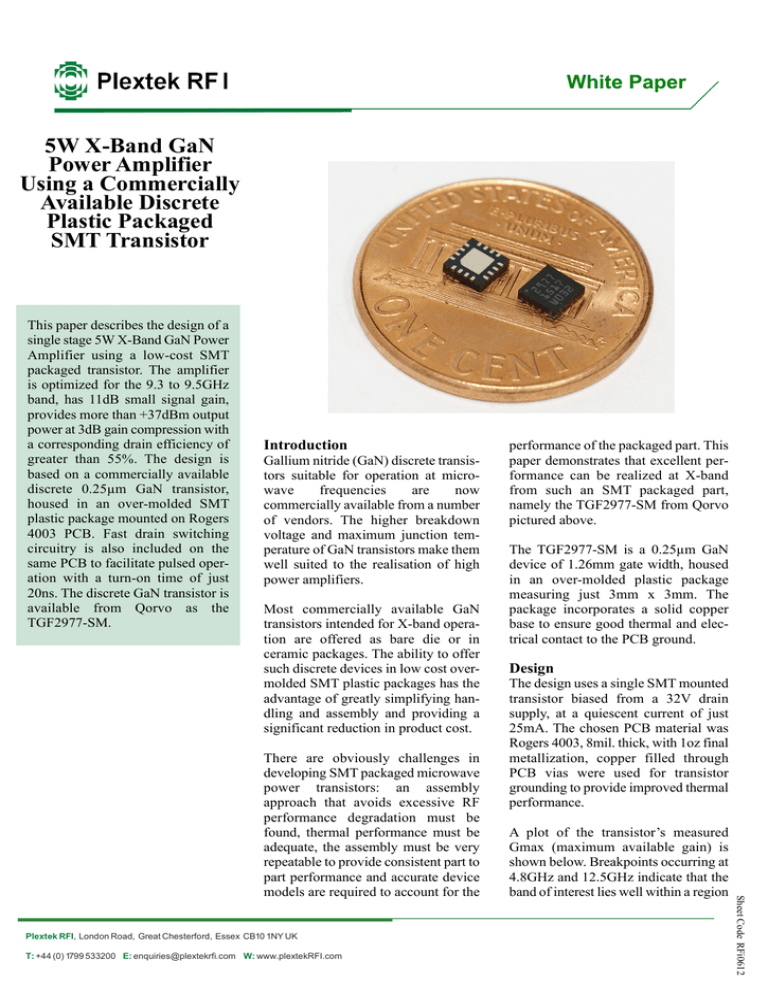
White Paper 5W X-Band GaN Power Amplifier Using a Commercially Available Discrete Plastic Packaged SMT Transistor This paper describes the design of a single stage 5W X-Band GaN Power Amplifier using a low-cost SMT packaged transistor. The amplifier is optimized for the 9.3 to 9.5GHz band, has 11dB small signal gain, provides more than +37dBm output power at 3dB gain compression with a corresponding drain efficiency of greater than 55%. The design is based on a commercially available discrete 0.25µm GaN transistor, housed in an over-molded SMT plastic package mounted on Rogers 4003 PCB. Fast drain switching circuitry is also included on the same PCB to facilitate pulsed operation with a turn-on time of just 20ns. The discrete GaN transistor is available from Qorvo as the TGF2977-SM. Introduction Gallium nitride (GaN) discrete transistors suitable for operation at microwave frequencies are now commercially available from a number of vendors. The higher breakdown voltage and maximum junction temperature of GaN transistors make them well suited to the realisation of high power amplifiers. Most commercially available GaN transistors intended for X-band operation are offered as bare die or in ceramic packages. The ability to offer such discrete devices in low cost overmolded SMT plastic packages has the advantage of greatly simplifying handling and assembly and providing a significant reduction in product cost. Plextek RFI, London Road, Great Chesterford, Essex CB10 1NY UK T: +44 (0) 1799 533200 E: enquiries@plextekrfi.com W: www.plextekRFI.com The TGF2977-SM is a 0.25µm GaN device of 1.26mm gate width, housed in an over-molded plastic package measuring just 3mm x 3mm. The package incorporates a solid copper base to ensure good thermal and electrical contact to the PCB ground. Design The design uses a single SMT mounted transistor biased from a 32V drain supply, at a quiescent current of just 25mA. The chosen PCB material was Rogers 4003, 8mil. thick, with 1oz final metallization, copper filled through PCB vias were used for transistor grounding to provide improved thermal performance. A plot of the transistor’s measured Gmax (maximum available gain) is shown below. Breakpoints occurring at 4.8GHz and 12.5GHz indicate that the band of interest lies well within a region Sheet Code RFi0612 There are obviously challenges in developing SMT packaged microwave power transistors: an assembly approach that avoids excessive RF performance degradation must be found, thermal performance must be adequate, the assembly must be very repeatable to provide consistent part to part performance and accurate device models are required to account for the performance of the packaged part. This paper demonstrates that excellent performance can be realized at X-band from such an SMT packaged part, namely the TGF2977-SM from Qorvo pictured above. Transistor Gmax of unconditional stability and that a maximum gain of around 14dB is available. The final amplifier gain will obviously be less than this due to losses associated with adding the matching and bias networks and the fact that the amplifier output will be power matched rather than conjugately matched. Although the device is unconditionally stable across the entire of X-band, at frequencies above 12.5GHz and below 4.8GHz it is potentially unstable so steps must be taken to ensure stability in these regions. There is also a significant amount of low frequency gain and it is good design practice to suppress this to avoid potential low frequency stability issues in the final amplifier. without affecting in-band performance. These components are used to provide lower frequency supply decoupling and stabilization and significantly reduce the low frequency gain. the SMT pads required for attachment of the transistor to the PCB. The amplifier schematic is shown below, all passive components are 0603. The bias networks for both the drain and gate make use of radial stubs which provide a short circuit at midband. This was the preferred means of implementing an RF short circuit as it offers better performance, tolerance and bandwidth compared to a shunt SMT capacitor. It also provides a convenient point at which other bias decoupling components can be added Large signal load pull data for the mounted device demonstrated that at 9.4GHz it is capable of delivering around 37.5dBm output power at 3dB compression. The target load impedance to present at the output reference plane was found to be 12.98Ω ­ j9.39Ω and the target source impedance to present at the input reference plane was found to be 11.64Ω ­ j55.75Ω. The reference planes are set at the edges of The short circuit provided by the radial stub is subsequently transformed to an open circuit by a narrow high impedance quarter wavelength line such that the drain and gate bias networks have almost no effect in-band. This offers some flexibility in where the bias networks are applied, convenient points in the distributed matching Vdd (Switched) Radial Stub Vgg Low Frequency Decoupling and Stabilisation RF Input DC Block Radial Stub λ/4 at 9.4GHz High Z Line λ/4 at 9.4GHz High Z Line Distributed Input Matching Network Low Frequency Decoupling and Stabilisation Distributed Output Matching Network TGF2977-SM Low Frequency Damping Circuit Plextek RFI, London Road, Great Chesterford, Essex CB10 1NY UK T: +44 (0) 1799 533200 E: enquiries@plextekrfi.com W: www.plextekRFI.com Simplified PA Schematic RF Output DC Block EM Simulated RF layout networks were chosen which were beneficial for both the layout and out of band performance. A damping circuit was employed at the input of the amplifier which was a further measure in ensuring low frequency stability and gain reduction. The circuit consists of two parallel short-circuited stubs in front of a parallel arrangement of a capacitor and a lossy inductor, formed by a resistor and two narrow lines. The position and topology of the circuit was carefully chosen to provide maximum low frequency rejection with minimum impact on in-band performance. An important feature of the topology is that it avoids presenting any undesirable impedance to the device which could lead to oscillation. The DC blocking capacitor employed at both the input and output was a high quality 0603 multi-layer component. 2-port s-parameter simulations were carried out on a corresponding model which included the effects of the mounting pads on the chosen substrate. The capacitor value was selected as that which gave the lowest in-band insertion loss. Input and output matching networks were implemented as, distributed 2section low pass structures. From the input reference plane moving backwards, the input matching network is essentially shunt C, series L, shunt C, series L. In a similar way, from the output reference plane moving forwards, the output matching network is essentially series L, shunt C, series L, shunt C. It is worth noting that an un-bonded pin was conveniently used as an open-circuit stub to form part of the first input shunt C. This is evident in the plot above which shows the layout of the final RF metal work. A photograph of the final assembled amplifier is shown below. The 8mil thick Rogers 4003 PCB is mounted onto an aluminum alloy T-carrier which in turn is mounted onto a heatsink. A fast drain switching circuit is provided on the same PCB. This area is coated in green solder resist which is omitted from the RF section. An end plate mounts onto the rear face of the T-carrier through which bias and control is applied. The blue wire is for the gate bias, the red wire for the drain bias, the yellow wire enables the drain switching and the black wire is 0V. The RF input and output have been Plextek RFI, London Road, Great Chesterford, Essex CB10 1NY UK T: +44 (0) 1799 533200 E: enquiries@plextekrfi.com W: www.plextekRFI.com designed to mate with edge-mount South West Microwave connectors. Note the hole in the front face of the T-carrier, this is to allow a thermocouple to be placed directly underneath the packaged device. Thermal analysis determined that the thermal resistance between the thermocouple and the package (through the PCB) was 8°C/W which allows the package temperature to be conveniently calculated for a given power dissipation. Measured Performance Small signal s-parameter measurements were carried out on the fully assembled amplifier at package base temperatures of -33°C, +25°C and +85°C. These measurements were carried out CW; the results are shown in the plot to the right. The s-parameter data demonstrates that the final amplifier has a small signal gain of around 11dB across the band which varies by around ±1.5dB over temperature. The input return loss is hardly affected by temperature and is better than 15dB across the band. The output return loss is nominally around 9.2dB (as the device was matched for power transfer and efficiency) and varies by around ±1dB over temperature. Large signal measurements were also carried out over temperature. These measurements were performed under pulsed conditions and utilized the on-board drain switching circuit, which provided a turn-on time of just 20ns. The duty cycle was 10% and the pulse width was 500µs. The RF envelope during the 500µs pulse is shown below for the amplifier running at 3dB compression at mid-band. Clean, fast edges are evident and there is very little power drop across the pulse period. Measured S-parameters of the PA During the large signal measurements, the input power was swept from around 10dB back-off, up to and slightly beyond, 3dB gain compression. Over the power sweep, the dissipated power in the package increases so the package temperature increases. In the following results, ‘low_temp’, ‘high_temp’ and ‘nom_temp’ refer to package base temperatures of -33°C, +85°C and +25°C respectively at the 3dB compression point. The presented results were taken at mid-band. Pulsed Output Envelope of the PA Plextek RFI, London Road, Great Chesterford, Essex CB10 1NY UK T: +44 (0) 1799 533200 E: enquiries@plextekrfi.com W: www.plextekRFI.com Curves are plotted to the right at low, nominal and high temperature. As with the small-signal measurements these reflect transistor base temperatures of -33oC, +25oC and +85oC. It can be seem that the mid-band output power at 3dB compression is nominally 37.1dBm, varying by just ±0.2dB over temperature. A plot of drain efficiency is also shown and demonstrates that at 3dB compression, the nominal drain efficiency is 57%, at low temperature it’s around 55% and at high temperature around 54%. Pout versus Pin of the PA The corresponding power added efficiency (PAE) at 3dB compression and nominal temperature is 48.5%. The PAE at low temperature is also around 48.5%, and is around 44% at high temperature. The final plot to the right summarizes the key performance metrics at 3dB compression and nominal temperature across the band of interest. Drain Efficiency versus Pin of the PA Summary This paper has demonstrated that excellent performance at X-band can be realized from a GaN transistor housed in an over-molded SMT plastic package such as the TGF2977-SM from Qorvo. A single stage power amplifier based on this device was designed for optimum performance from 9.3 to 9.5GHz. At mid-band under nominal conditions, the amplifier has over 11dB small signal gain, provides over 37dBm output power at 3dB compression with a corresponding drain efficiency of 57%. Large-signal Performance Summary of the PA Plextek RFI, London Road, Great Chesterford, Essex CB10 1NY UK T: +44 (0) 1799 533200 E: enquiries@plextekrfi.com W: www.plextekRFI.com


