Three Balun Designs for Push-Pull Amplifiers Application Note
advertisement

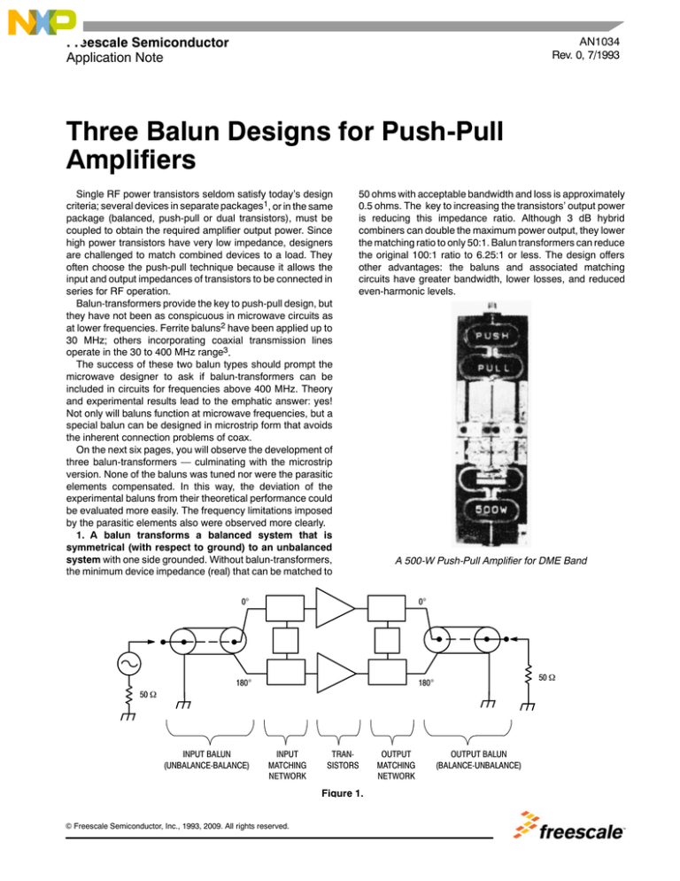
Freescale Semiconductor Application Note AN1034 Rev. 0, 7/1993 Three Balun Designs for Push-Pull Amplifiers Single RF power transistors seldom satisfy today’s design criteria; several devices in separate packages1, or in the same package (balanced, push-pull or dual transistors), must be coupled to obtain the required amplifier output power. Since high power transistors have very low impedance, designers are challenged to match combined devices to a load. They often choose the push-pull technique because it allows the input and output impedances of transistors to be connected in series for RF operation. Balun-transformers provide the key to push-pull design, but they have not been as conspicuous in microwave circuits as at lower frequencies. Ferrite baluns2 have been applied up to 30 MHz; others incorporating coaxial transmission lines operate in the 30 to 400 MHz range3. The success of these two balun types should prompt the microwave designer to ask if balun-transformers can be included in circuits for frequencies above 400 MHz. Theory and experimental results lead to the emphatic answer: yes! Not only will baluns function at microwave frequencies, but a special balun can be designed in microstrip form that avoids the inherent connection problems of coax. On the next six pages, you will observe the development of three balun-transformers — culminating with the microstrip version. None of the baluns was tuned nor were the parasitic elements compensated. In this way, the deviation of the experimental baluns from their theoretical performance could be evaluated more easily. The frequency limitations imposed by the parasitic elements also were observed more clearly. 1. A balun transforms a balanced system that is symmetrical (with respect to ground) to an unbalanced system with one side grounded. Without balun-transformers, the minimum device impedance (real) that can be matched to 50 ohms with acceptable bandwidth and loss is approximately 0.5 ohms. The key to increasing the transistors’ output power is reducing this impedance ratio. Although 3 dB hybrid combiners can double the maximum power output, they lower the matching ratio to only 50:1. Balun transformers can reduce the original 100:1 ratio to 6.25:1 or less. The design offers other advantages: the baluns and associated matching circuits have greater bandwidth, lower losses, and reduced even-harmonic levels. A 500-W Push-Pull Amplifier for DME Band 0 0 180 50 180 50 INPUT BALUN (UNBALANCE-BALANCE) INPUT MATCHING NETWORK TRANSISTORS OUTPUT MATCHING NETWORK OUTPUT BALUN (BALANCE-UNBALANCE) Figure 1. Freescale Semiconductor, Inc., 1993, 2009. All rights reserved. RF Application Information Freescale Semiconductor AN1034 1 2. Baluns are not free of disadvantages. Coupling a pair of push-pull amplifiers with 3-dB hybrids avoids (for four-transistor circuits) one of these: the higher broadband VSWRs of balun-transformers. A second disadvantage, the lack of isolation between the two transistors in each push-pull configuration, is outweighed by the advantages of the balun design in reducing the critical impedance ratio. 3. In this simple balun that uses a coaxial transmission line, the grounded outer conductor makes an unbalanced termination, and the floating end makes a balanced termination. Charge conservation requires that the currents on the center and the outer conductors maintain equal magnitudes and a 180-degree phase relationship at any point along the line. By properly choosing the length and characteristic impedance, this balun can be designed to match devices to their loads. In the case shown, if A = 90 degrees, the matching condition is: ZA2 = 2 x R x 50. INPUT (LOW VSWR) QUAD-RATURE COMBINER 4. By adding a second coaxial line, the basic balun can be made perfectly symmetrical. In this symmetrical coaxial balun, the bandwidth (in terms of the input VSWR) is limited by the transformation ratio, 50/2R, and the leakages, which are represented by lines B and C. If ZA = 50 ohms and R = 25 ohms, the bandwidth is constrained only by the leakages. Experimental Version of a Simple Balun Using Coaxial Lines 0 0 -- 90 -- 90 50 50 QUAD-RATURE COMBINER OUTPUT (LOW VSWR) Figure 2. 50 LINE A LINE B V R --V R LINE A: ZA, A LINE B, LINE C: ZB = ZC; B = C (a) COAXIAL BALUN DESIGN 1 R 50 LINE A ZP R LINE C R LINE A: ZA, A LINE B: ZB, B ZP = jZB TAN B AND ZP & R 50 LINE A R LINE B (b) EQUIVALENT CIRCUIT SYMMETRICAL COAXIAL BALUN (DESIGN 1) Figure 4. Figure 3. AN1034 2 RF Application Information Freescale Semiconductor 5. The equivalent circuit for the symmetrical balun shows the effect of the leakages (lines B and C) on its performance. A broadband balun can be obtained by using a relatively high characteristic impedance for these leakage lines. In theory, the construction of the baluns insures perfect balance. LINE C 50 R R LINE A LINE B SYMMETRICAL BALUN EQUIVALENT CIRCUIT Figure 5. 6. The symmetric balun’s input equivalent circuit further simplifies its configuration and allows the input VSWR to be calculated.4 In this design, line A has a characteristic impedance of ZA = 50 ohms, a length of LA = 1799 mils, and a dielectric constant (relative) of r = 2.10. For lines B and C, Z0 = 30 ohms, L = 1799 mils, and eff = 2.23. LINE BB 50 LINE AA RL LINE AA: ZAA = ZA; AA = A LINE BB: ZBB = 2ZB; BB = B RL = 2R SYMMETRIC BALUN INPUT EQUIVALENT CIRCUIT Figure 6. 7. The theoretical input VSWR has been calculated for 50-ohm values of ZA and 2R, and for two other sets of values for these parameters. The performance of an experimental balun will be compared with these theoretical results. 3:1 INPUT VSWR 2.5:1 2:1 ZA = 25 2R = 12.5 ZA = 10 2R = 2 1.5:1 ZA = 50 1:1 2R = 50 0.7 0.8 0.9 1.0 1.1 1.2 1.3 FREQUENCY -- GHz 1.4 1.5 THEORETICAL INPUT RESPONSE OF THE SYMMETRIC BALUN (DESIGN 1) Figure 7. AN1034 RF Application Information Freescale Semiconductor 3 measurement system. The balun was tested from 0.6 to 1.5 GHz. 8. Two /16 line-section Chebyshev impedance transformers match the experimental balun to a 50-ohm 25 LINE C LINE D LINE E LINE F LINE D LINE E LINE F R LINE A LINE B 50 R 25 BALUN COAXIAL/ MICROSTRIP 25 LINES MICROSTRIP LOAD /16 LINE-SECTION CHEBYSHEV IMPEDANCE TRANSFORMER MICROSTRIP FOR LINE A: Zo = 50 L = 1799 MILS; r = 2.10 LINES B AND C: Zo = 30 L = 1799 MILS; eff = 2.23 LINES D AND D: Zo = 25 L = 750 MILS; eff = 2.23 LINES E AND E: Zo = 61.5 ; L = 464 MILS; eff = 2.10 LINES F AND F: Zo = 20.3 ; L = 441 MILS; eff = 2.31 EXPERIMENTAL COAXIAL BALUN (DESIGN 1) WITH OUTPUT TRANSFORMERS PHASE DIFFERENCE -- DEGREES 9. The measured phase difference and insertion loss difference, which indicate the maximum unbalance for the Design 1 experimental balun, are 3 degrees and 0.2 dB, respectively. 185 INSERTION LOSS DIFFERENCE -- dB Figure 8. 0.5 180 175 0 --0.5 0.6 0.7 0.8 0.9 1.0 1.1 1.2 1.3 1.4 1.5 FREQUENCY -- GHz BALUN MEASURED PERFORMANCE FOR DESIGN 1 Figure 9. 2:1 INPUT VSWR 10. The maximum VSWR measured for the first design is 1.5:1. Note the comparison between the calculated and measured response. The performance shown can be considered valid for amplifier applications up to an octave range. 1.5:1 1:1 0.6 0.7 0.8 0.9 1.0 1.1 1.2 1.3 1.4 FREQUENCY -- GHz CALCULATED MEASURED 1.5 BALUN PERFORMANCE FOR DESIGN 1 Figure 10. AN1034 4 RF Application Information Freescale Semiconductor 11. The second balun design adds two identical coax lines to the simple balun just described. The inputs of the identical lines are connected in series to the output of the first balun. By putting their outputs in parallel, the final output becomes symmetrical. The output impedance is halved. 50 LINE C LINE G LINE F LINE A LINE D LINE B LINE E R R FIRST SECTION SECOND SECTION LINE B AND LINE C: IDENTICAL LINE D AND LINE F: IDENTICAL LINE E AND LINE G: IDENTICAL COAXIAL BALUN DESIGN 2 Figure 11. 12. The equivalent circuit for the Design 2 balun indicates that its bandwidth, in terms of input VSWR, is limited by the transformation ratios of the first and second sections and the leakages represented by lines B, C, E, and G. If the balun is designed with ZA = 50 ohms, and ZD = ZF = 25 ohms, and if the load, 2R, is set at 2 x 6.25 ohms, all of the transmission lines will be connected to their characteristic impedances. In this case, the bandwidth will be limited by the leakage alone, and a broadband balun can be obtained by choosing lines B, C, E, and G with relatively high impedance and /4 length for the center frequency. The balun achieves a transformation from 50 ohms to twice 6.26 ohms without causing a standing wave in the coaxial cables. LINE C LINE E 0 0 LINE F LINE A R H I R 50 LINE D 180 180 LINE B LINE G DESIGN 2 BALUN EQUIVALENT CIRCUIT Figure 12. 2.5:1 INPUT VSWR 13. The performance of the Design 2 balun can be calculated using its equivalent circuit. The calculated VSWR shows a response very close to the simple coaxial balun (Figure 10) because the new second section has four times the bandwidth of the first section. This design and its two companions are intended to have octave bandwidths centered at 1.1 GHz, the central frequency used in distance measuring equipment (DME, 1.025 to 1.150 GHz) and tactical air navigation (TACAN, 0.960 to 1.215 GHz). For line A: ZA = 50 ohms, LA = 1799 mils, r = 2.10; for lines B, C, E, and G: Z0 = 30 ohms, L = 1799 mils, eff = 2.23; lines D and F: Z0 = 25 ohms, L = 1799 mils, r = 2.10. 2:1 1.5:1 1:1 0.7 0.8 0.9 1.0 1.1 1.2 1.3 1.4 1.5 FREQUENCY -- GHz THEORETICAL INPUT RESPONSE OF THE COAXIAL BALUN (DESIGN 2) Figure 13. AN1034 RF Application Information Freescale Semiconductor 5 14. Two /4 transformers match the experimental two--sectlon coaxial balun’s 6.26-ohm impedance to the 50-ohm load. Although these transformers drastically reduce the bandwidth (in terms of the VSWR), they don’t affect the balance. Two-section balun often used in the 100- to 400-MHz range 6.25 LINE C LINE G LINE F LINE H LINE A 50 LINE D LINE H LINE B 50 LINE I LINE Z 50 LINE E 6.25 FIRST SECTION CONNECTION 25 LINES MICROSTRIP SECOND SECTION LOAD /4 TRANSFORMER MICROSTRIP FOR LINE A: ZA = 50; L = 1799 MILS; r = 2.1 LINES B AND C: ZB = ZC = 30 ; L = LC = 1799 MILS; eff = 2.23 LINES D AND F: ZD = ZF = 25 ; LD = LF = 1799 MILS; r = 2.1 LINES E AND G: ZE = ZG = 30 ; LE = LG = 1799 MILS; eff = 2.23 LINES H AND H: ZH = ZH = 25 ; LH = LH MILS; eff = 2.23 LINES I AND I: ZI = ZI = 17.7 ; LI = LI = 1772 MILS; eff = 2.30 EXPERIMENTAL BALUN (DESIGN 2) WITH TRANSFORMERS INSERTION LOSS DIFFERENCE -- dB 15. The measured phase difference and measured insertion loss difference are plotted for the two-section coaxial balun (Design 2). The maximum unbalances for these two measurements over the octave bandwidth are 1 degree and 0.2 dB. PHASE DIFFERENCE -- DEGREES Figure 14. 185 180 175 0.5 0 --0.5 0.7 0.8 0.9 1.0 1.1 1.2 1.3 FREQUENCY -- GHz DESIGN 2 BALUN MEASURED PERFORMANCE 1.4 Figure 15. AN1034 6 RF Application Information Freescale Semiconductor 3:1 2.5:1 INPUT VSWR 16. The calculated and measured values for the input VSWR for the Design 2 balun show close agreement between the experimental and predicted performances. This indicates that the parasitic inductors at the connections are negligible to at least 1.4 GHz. Moreover, the balun has excellent balance to 1.4 GHz and achieves the 4:1 transformation without causing a standing wave in the coaxial line. Despite the many excellent qualities of the Design 1 and Design 2 baluns, the necessary coaxial line connection limits them to approximately 2 GHz. 2:1 1.5:1 1:1 0.7 0.8 0.9 1.0 1.1 1.2 1.3 FREQUENCY -- GHz :CALCULATED :MEASURED 1.4 DESIGN 2 BALUN PERFORMANCE Figure 16. 17. The problems associated with the previous coaxial baluns can be reduced or eliminated by using a balun that allows a microstrip coplanar arrangement of the input and output lines, which greatly simplifies the connections to the amplifier. This balun5 consists of an input line, A, connected in series to three elements in the center of the half-wavelength cavity: a reactive open-circuit stub, B, and the /4 output lines, C and D. CAVITY OUTPUT E (0) BALUN JUNCTION LINE C LINE D LINE A LINE B LINE F LINE E E (180) /4 INPUT OUTPUT /4 ZC = ZD AND ZE = ZF DESIGN 3 COAXIAL BALUN Figure 17. 18. The equivalent circuit of the Design 3 coaxial version balun shows lines C and D connected to place their input signals in antiphase, thereby producing two antiphase signals at their outputs. Transmission line impedances and lengths are optimized to achieve the correct input/output transformation ratio and a good match across the desired bandwidth. If only one frequency or a narrow bandwidth is desired, and all lengths are /4, the matching condition ZA2/50 = 2ZC2/R, will occur. In this case, ZE (ZE = ZF) and ZB have no significance except for loss. LINE F LINE B LINE E LINE A 50 LINE D R LINE C R E (180) E (0) BALUN EQUIVALENT CIRCUIT (DESIGN 3) Figure 18. AN1034 RF Application Information Freescale Semiconductor 7 19. The coplanar arrangement of input and output lines can be accomplished with mlcrostrip technology. The uppermost conductor plane contains input line A, output lines C and D, and the open stub B. Coupling between these lines is avoided by separating them by at least one line width. The middle conductor carries the ground plane for the lines. To avoid radiation loss, the center conductor must extend at least one line width to either side of the upper plane circuit line. The balun resonant cavity is formed by the region between the middle and the lower conductor planes. A hole for the cavity is cut in the circuit fixture, filled with dielectric, and covered with the middle conductor plane. The end-to-end length of the cavity is nominally a half-wavelength at midband. To avoid disturbance of the field distribution, the cavity width must be at least three times the width of the middle conductor plane. The arms of the balun cavity are folded to produce two parallel and proximate output transmission lines. This configuration is more suited to coupling two transistors than the original layout in which the two outputs were on opposite sides (Figure 17). MIDDLE CONDUCTOR PLANE LINE A INPUT LINE C MIDDLE CONDUCTOR PLANE /4 LINE E E (180) OUTPUT BALUN JUNCTION CIRCUIT FIXTURE E (0) OUTPUT LINE F /4 LINE B LINE D CAVITY CIRCUIT DIELECTRIC CAVITY DIELECTRIC MICROSTRIP BALUN (DESIGN 3) Figure 19. 20. The input equivalent circuit for the microstrip version of the Design 3 balun allows its theoretical performance to be calculated. The design parameters shown provide a microstrip circuit that can be compared with the coaxial baluns of Design 1 and Design 2. Transmission line A and lines C and D are loaded by their characteristic impedances — in this case, 50 and 25 ohms. The cavity and the stub impose the principal frequency limitation. The impedances of these elements are dictated by the properties of the available dielectric substrates (glass-Teflon 0.020 and 0.0625 inches thick). LINE CC LINE BB LINE AA LINE DD RL FOR LINE AA: ZA = 50 ; L 1888 MIL; ff = 2.10 LINE BB: ZB = 25 ; L 1810 MIL; eff = 2.23 LINE CC: 2ZE = 35.8 ; LE = 1772 MIL; ff = 2.33 LINE DD: 2ZD = 50 ; LD 1546 MIL; eff = 2.23 RL 2 X R = 50 INPUT EQUIVALENT CIRCUIT (DESIGN 3 BALUN) Figure 20. AN1034 8 RF Application Information Freescale Semiconductor 21. The input VSWR can be calculated based on the equivalent circuit for the microstrip balun. For a oneoctave bandwidth, the input VSWR is lower than 1.75:1. This calculated performance is similar to that of the two previous balun designs. The design of the microstrip has theoretically perfect balance. INPUT VSWR 2.5:1 2:1 1.5:1 1:1 0.7 0.8 0.9 1.0 1.1 1.2 1.3 1.4 1.5 FREQUENCY -- GHz THEORETICAL INPUT VSWR OF MICROSTRIP BALUN (DESIGN 3) Figure 21. 22. The equivalent circuit of the microstrip balun shows the balun during performance measurements with /16 matching lines. The experimental model uses 18-mil glass-Teflon (r = 2.55) for the tap circuits and 62.5 mil glass-Teflon for the cavity. Balance properties were measured with a 50-ohm system, which was transformed to 25 ohms by the /16 line section, Chebyshev impedance transformers which have a bandwidth from 0.960 to 1.215 GHz. The Experimental Microstrip Balun Showing the Uppermost Conductor Plane LINE F LINE B LINE D LINE A 50 LINE C BALUN LINE G LINE I LINE K R = 50 LINE H LINE J LINE L R = 50 25 /16 TRANSMISSION LINE-SECTION LINE TRANSFORMER FOR LINE A: Zo = 50 ; L = 1888 MILS; ff 2.10 LINE B: Zo = 25 ; L = 1810 MILS; ff 2.23 LINES E AND F: Zo = 30 ; L = 1772 MILS; eff 2.33 LINES C AND D: Zo = 25 ; L = 1546 MILS; eff 2.23 LINES G AND H: Zo = 25 ; L = 140 MILS; ff 2.23 LINES I AND J: Zo = 61.1 ; L = 466 MILS; eff 2.07 LINES K AND L: Zo = 20.5 ; L = 443 MILS; eff 2.31 EQUIVALENT CIRCUIT MICROSTRIP BALUN (DESIGN 3) WITH TRANSFORMERS Figure 22. AN1034 RF Application Information Freescale Semiconductor 9 PHASE DIFFERENCE -- DEGREES INSERTION LOSS DIFFERENCE -- dB 23. The unbalance between output ports for a one-octave bandwidth is shown in the measured 1.5 degree maximum phase difference and 0.15-dB maximum insertion loss difference. DESIGN 3 BALUN MEASURED PERFORMANCE 185 180 175 0.5 0 --0.5 0.6 0.7 0.8 0.9 1.0 1.1 1.2 FREQUENCY -- GHz 1.3 1.4 1.5 0.9 1.0 1.1 1.2 1.3 1.4 FREQUENCY -- GHz CALCULATED MEASURED 1.5 Figure 23. 2.5:1 INPUT VSWR 24. The central frequency is 10 percent higher than expected, but response is close to the calculated values if relative frequency is considered. If the output transformers and their effect on input VSWR are disregarded, an octave bandwidth with a maximum input VSWR of around 2.0:1 can be obtained. The 100 MHz shift between the two curves may be caused by the improper determination of the folded cavity’s electrical length. Similar calculation inaccuracies may arise from effects at the balun junction and from the electrical length of the stub. As in the calculated response, the experimental microstrip balun performs comparably to the two coaxial designs. 2:1 1.5:1 1:1 0.6 0.7 0.8 DESIGN 3 BALUN PERFORMANCE Figure 24. 25. The similarity in the performance of the three balun designs within the considered frequency bands indicates that the parasitic elements do not significantly affect the theoretical properties. The frequency limit is higher than 1.5 GHz for all three. In the 0.960-to-1.215-GHz bandwidth (TACAN and DME applications), each performed with satisfactory balance. The table compares the main characteristics of the balun designs. The phase differences ( 1.5 degrees) for all three baluns are similar to those experienced with the miniature 3-dB hybrid couplers that are normally used to combine transistors for microwave balanced amplifiers. But the insertion loss differences of the baluns are better-0.2 dB for a one-octave bandwidth compared with 0.5 dB. The physically simple microstrip balun eliminates the connection problem inherent in coaxial designs: physical variances that breed standing waves and unbalance. Microstripping the transmission lines allows a designer to choose any value of characteristic impedance of the lines. Consequently, the microstrip balun is both more manageable and more controllable. Since the balun load impedance will vary with frequency, the best results will be obtained by simultaneously optimizing the balun parameters with those of the matching network. The transistor’s internal prematching network must be considered. Maximum Experimental Unbalance For One-Octave Bandwidth Theoretical Input VSWR For: Balun Loads, R (ohms) MAG (dB) 960 -- 1215 MHz One-Octave Bandwidth Coaxial I (Design 1) 25 3 0.2 1.15:1 1.6:1 Coaxial II (Design 2) 6.25 1 0.2 1.15:1 1.6:1 Microstrip (Design 3) 25 1.5 0.2 1.20:1 1.8:1 Type of Balun Figure 25. Performance of the Three Balun Designs AN1034 10 RF Application Information Freescale Semiconductor References 1. “35/50 Watt Broadband (160 -- 240 MHz) Push-Pull TV Amplifier Band III,” TRW Application Note, TRW RF Semiconductors Catalog No. 97, p. 84AN. 2. “150 W Linear Amplifier 2 to 28 MHz, 13.5 Volt DC,” TRW Application Note, TRW RF Semiconductors Catalog No. 97, p. 108AN. 3. TRW Application Notes on the TPM-4100 (100 W, 100 -400 MHz); the TPM-4040 (40 W, 100 -- 400 MHz); the TPV-3100 (110 W, Band III); and the TPV-5050 (50 W, UHF) available from TRW RF Semiconductors. 4. The program used for the circuit calculation was COMPACT (Computerized Optimization of Microwave Passive and Active Circuits). 5. Gordon J. Laughlin, “New Impedance-Matched Wideband Balun and Magic Tee,” IEEE Transactions: Microwave Theory and Technology, Vol. MTT-24, No. 3, (March 1976). AN1034 RF Application Information Freescale Semiconductor 11 How to Reach Us: Home Page: freescale.com Web Support: freescale.com/support Information in this document is provided solely to enable system and software implementers to use Freescale products. There are no express or implied copyright licenses granted hereunder to design or fabricate any integrated circuits based on the information in this document. Freescale reserves the right to make changes without further notice to any products herein. Freescale makes no warranty, representation, or guarantee regarding the suitability of its products for any particular purpose, nor does Freescale assume any liability arising out of the application or use of any product or circuit, and specifically disclaims any and all liability, including without limitation consequential or incidental damages. “Typical” parameters that may be provided in Freescale data sheets and/or specifications can and do vary in different applications, and actual performance may vary over time. All operating parameters, including “typicals,” must be validated for each customer application by customer’s technical experts. Freescale does not convey any license under its patent rights nor the rights of others. Freescale sells products pursuant to standard terms and conditions of sale, which can be found at the following address: freescale.com/SalesTermsandConditions. Freescale and the Freescale logo are trademarks of Freescale Semiconductor, Inc., Reg. U.S. Pat. & Tm. Off. All other product or service names are the property of their respective owners. E 1993, 2009 Freescale Semiconductor, Inc. AN1034 AN1034 Rev. 0, 7/1993 12 RF Application Information Freescale Semiconductor


