Q Q v -
advertisement
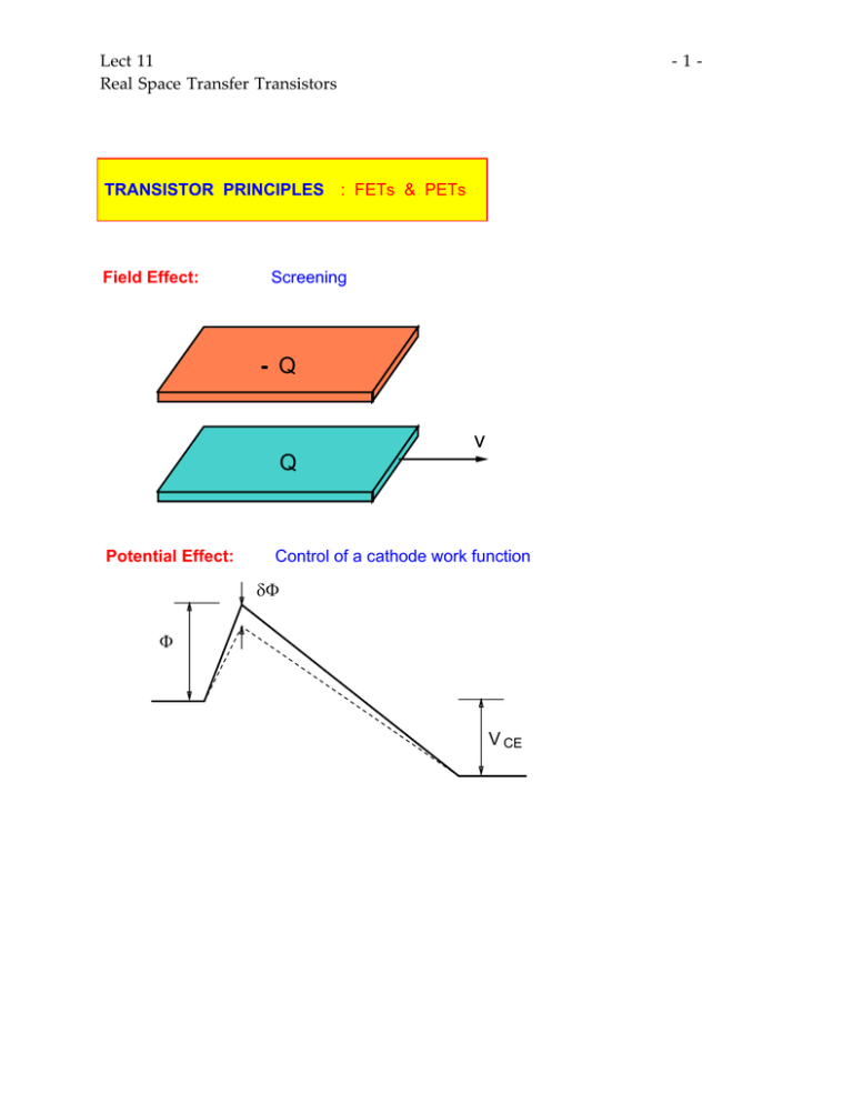
Lect 11 Real Space Transfer Transistors -1- TRANSISTOR PRINCIPLES : FETs & PETs Field Effect: Screening - Q v Q Potential Effect: Control of a cathode work function δΦ Φ V CE Lect 11 Real Space Transfer Transistors -2- FETs: - Q I = Qv v L Q L "Biblical" principle: "Transit time" limitation : τ > Q in I out = L v Q for Q I for I Lect 11 Real Space Transfer Transistors -3- PETs ’ ’ δΦ Φ V CE − Φ /kT Ι ~ e δΦ ~ δ Q τ ~ Ι -1 in Speed increases with current until exponential law fails at high currents PET τ FET (space-charge effect) limited by transit time across Lect 11 Real Space Transfer Transistors -4- Charge Injection Transistor (CHINT) Operating principle: ΙA Control of cathode temperature T3 Anode T2 T1 Cathode VA ΙA Cathode Heater VA3 Heating Voltage VA2 VA1 S D T Emitter Barrier Hot-electron cathode Collector C Lect 11 Real Space Transfer Transistors Ballistic Electrons & -5- Hot Electrons Distribution f (E) f (E) ~ e - E/kT e f (E) ~ δ (E-E 0 ) kTe E0 energy MOMOM E SMS ( THETA ) IBT HBT Ballistic Transistors Lect 11 Real Space Transfer Transistors -6- Real Space Transfer + + + + + + + + I DRAIN V SOURCE Ballistic Electrons & Hot Electrons f (E) ~ e Distribution f (E) kTe - E/kT e f (E) ~ δ (E-E 0 ) E0 energy E Lect 11 Real Space Transfer Transistors -7- CHINT Structures 1984: n AlGaAs S D GaAs AlGaAs COLLECTOR n GaAs VC 1990: S D o 300 A C o InGaAs n + InGaAs n - Emitter 500 A Barrier 2000 A InAlAs Collector ~ 1 µm InGaAs o u n+ Lect 11 Real Space Transfer Transistors P.Mensz, P.Garbinski, A.Cho, D.Sivco, S.Luryi Appl. Phys. Lett. 57 , 2563 (1990) InGaAs/InAlAs CHINT S -8- D L CH g h f e d BARRIER c C b a COLLECTOR Semi-insulating InP substrate o a: 5000 A InGaAs b: 500 A InGaAs 19 n ( Si: 10 n ( Si: 10 17 ) o ) o e: 25 A f: 200 A InGaAs o o c: 2000 A InAlAs 500 A InGaAs n ( Si: 10 19 ) n ( Sn: 10 20 ) o ( Si: 10 16 ) h: Si 3 N 4 5 10 T = 300 K W = 25 µ m 4 3 1 µm S 8 D 2 6 4 C 1 0 2 4 + 3.9 V 6 Heating Voltage VD 8 2 10 Collector Current (mA) Drain Current (mA) n g: 500 A Ti / 1000 A Au u o d InAlAs o Lect 11 Real Space Transfer Transistors -9- Hot-Electron Instabilities in CHINT k o 0 q p -1 u -2 all stable states -3 d -4 -1.0 -0.5 0.0 0.5 1.0 Source-Drain Voltage (V) 1.5 2.0 2.0 u Potential, V Drain Current (A/cm) 1 1.5 t s 1.0 V D 0.5 k 0.0 0 S 1 2 3 Distance, um 4 5 D Lect 11 Real Space Transfer Transistors - 10 - Broken Symmetry States in CHINT S. Luryi and M. Pinto Phys. Rev. Lett. 67 , 2351 (1991) k o 0 s a b -1 t Multiply-connected I - V characteristics c u -2 VC = 2V 7 v sat = 10 cm/s dB -3 = 0.2 um L ch = 5 um d -4 -1.0 -0.5 0.0 0.5 1.0 Source-Drain Voltage (V) 1.5 2.0 Anomalous collector-controlled states at V DS = 0 Electron Temperature (eV) Drain Current (A/cm) 1 0.15 a d b c 0.10 0.05 + VC 0.00 0 1 2 3 4 Source-Drain Distance (um) 5 Lect 11 Real Space Transfer Transistors - 11 - Broken Symmetry States in CHINT a b -1 Anomalous collector-controlled states at V DS = 0 k o 0 s t c u -2 -3 d -4 -1.0 -0.5 Electron Temperature (eV) Drain Current (A/cm) 1 0.0 0.5 1.0 Source-Drain Voltage (V) 0.15 1.5 2.0 + VC d a d b c 0.10 0.05 0.00 0 1 2 3 4 Source-Drain Distance (um) 5 Lect 11 Real Space Transfer Transistors - 12 - Evolution of non-stationary states 1 Drain Current (A/cm) Collector Current (A/cm) 8.0 6.0 4.0 k o 0 s a b -1 t c - + u -2 V = 2V C 2.0 -3 d 0.0 -4 0 10 20 30 -1.0 40 Time (ps) -0.5 0.0 0.5 1.0 Source-Drain Voltage (V) 1.5 Electron Temperature (eV) 0.6 0.4 ab+ c+ d a+ bc- o 0.2 0.0 0 1 2 3 Source-Drain Distance (um) 4 5 2.0 Lect 11 Real Space Transfer Transistors - 13 - 8.0 2 2V 6.0 VC 4.0 1V 2.0 + VC Potential (V) collector Current (A/cm) Realization of anomalous states by rapid ramping of V C 1 0.0 0 10 20 30 40 50 τcr t (ps) 0 0 Critical ramping speed is determined by the rate at which the increasing fringing field ( ~ dVC /dt ) is screened by channel electrons ( ~ vsat ) VSD 100 612 311 312 212 321 322 10 linear quadratic 1 2 3 4 5 100 Critical ramping time (ps) Critical ramping time (ps) τcr 1 Source-Drain Distance (um) L ch = 5 um 75 Db = 0.2 um vsat = 107cm/s 50 25 V = 1.211 V cr 0 1 10 Channel length (um) 0 1 2 3 4 5 Endramp voltage Vmax (V) 6 Lect 11 Real Space Transfer Transistors - 14 - Formation of Hot-Electron Domains Drain Current (A/cm) 1 k o 0 q p -1 u -2 all stable states -3 d -4 -1.0 -0.5 0.0 0.5 1.0 Source-Drain Voltage (V) 1.5 2.0 Potential, V u 1.5 t s 1.0 V D 0.5 k 0.0 0 1 2 3 Distance, um 4 5 2.0 Lect 11 Real Space Transfer Transistors - 15 - P.Mensz, H.Schumacher, P.Garbinski, A.Cho, D.Sivco, S.Luryi IEDM Tech. Digest, p. 395 (1990) Microwave Studies of CHINT 25 25 IC Drain Current (mA) 20 20 VD = 0.8 V S12 15 x 10 15 S 21 2 S/mm 1 10 2 3 10 s S 5 S11 22 5 ID 0.5 - 25.5 GHz 0 0 1 2 3 4 Heating Voltage V D (V) 20 h 21 10 20 MSG /de dB 5 c Small-Signal Gain (dB) 15 VC = 4.0 V VD = 0.8 V MAG 0 L = 0.8 µm W = 25 µm -5 0 1 10 Frequency (GHz) 100 Collector Current (mA) VC = 4.0 V Lect 11 Real Space Transfer Transistors - 16 - Microwave Performance of top-collector CHINT G. Belenky, P. Garbinski, P. Smith, S. Luryi A. Y. Cho, R. A. Hamm, D. L. Sivco (1993) Current Gain (dB) T = 300 K c /de dB 20 40 InGaAs/InP 30 20 InGaAs/InAlAs 10 0 1 10 Frequency (GHz) 100 Lect 11 Real Space Transfer Transistors - 17 - Speed Limits of CHINT Limiting mechanisms: S D o 2000 A a. Establishment of hot-electron ensemble Phonons: ~ 1 ps e-e interaction < 1ps (if concentration not too low) b. Charging time C transit over high-field regions ~ 2-3 ps f T ~ 80 - 50 GHz c. Parasitic C-D capacitance presently dominates C Collector-top CHINT preferable S K. Maezawa and T. Mizutani, Jpn. J. Appl. Phys. 30, 1190 (1991) D CHINT vs FET "FET like" but not limited by time of flight S->D in small-signal operation Lect 11 Real Space Transfer Transistors - 18 - Physical Picture Hot electron ensemble equilibrates via e-e interaction RST is due to electrons in high-energy tails of the distribution function Tails are repolutated "instantaneously" from the main part of distr. (at high enough conc.) The effective temperature of electrons is determined by energy balance Te ρ Te = f ( | VSD | ) Te can be very high, more than 1000 K The fundamental symmetry of charge injection by RST Ε Φ D S Can interchange S D collector current will not change ! C Lect 11 Real Space Transfer Transistors - 19 - CHINT logic S.Luryi, P.Mensz, M.Pinto, P.Garbinski, A.Cho, D.Sivco Appl. Phys. Lett. 57 , 1787 (1990) S D EMITTER BARRIER S D IC OUT 0 0 low 1 0 1 high 0 1 0 high 0 1 1 low 1 COLLECTOR OUT RL XNOR ( S , D ) V CC S n+ n- D EMITTER u BARRIER p ACTIVE REGION p+ L = XOR ( S , D ) COLLECTOR C Lect 11 Real Space Transfer Transistors - 20 - Light-Emitting CHINT S. Luryi, Appl. Phys. Lett. 58, 1727 (1990) RST of electrons into a complementary collector EC Equilibrium EV EF Flat bands VFB RST Operating regime VC hν Lect 11 Real Space Transfer Transistors S Light-emitting logic RST device D n+ n- - 21 - EMITTER u BARRIER p ACTIVE REGION p+ L = XOR ( S , D ) COLLECTOR C Mastrapasqua et al Appl. Phys. Lett. 60, 2415 (1992) IEEE TED-40, 250 (1993) d S D a c L ch b o 500 A InGaAs channel n (Si: 10 17 ) InAlAs barrier (undoped) o 2000 A C e o InGaAs collector active layer 500 A 1µm p (Be: 10 17 ) p (Be: 3x10 18 ) InAlAs collector confinement layer InP semi-insulating substrate o a: 200 A InGaAs, n (Sn: 10 20 ) o b: 25 A InAlAs, o c: 2500 A Si 3N 4 n (Sn: 10 19 ) o o d: 300 A Ti / 1800 A Au o o e: 800 A AuBe / 2000 A Au Lect 11 Real Space Transfer Transistors - 22 - Light = xor ( S , D ) VD (V) Vc = 3 V VS (V) 1.5 Time 0 1-0 1-1 0-1 0-0 1.5 0 Light Output PL (µW) 1 T = 290 K 0.24 0 6x10 -3 0.21 1 T = 235 K 0.43 0.36 3x10 -4 0 3x10 -2 7x10 -3 1.45 0.98 T = 100 K 1 < 10-4 < 10-4 0 Out : 1 0 1 0 Lect 11 Real Space Transfer Transistors - 23 - Current = xor ( S , D ) Vc = 3 V VD (V) 1.5 0 VS (V) 1.5 0 Time 1-0 1-1 0-1 0-0 Collector Current I C (mA) 2.5 2 1.87 1.81 T = 290 K 1 0.4 0 0.98 0.87 1 1.14 T = 235 K 0.06 0 1 0.52 5x10 -8 0.36 T = 100 K 2x10 0 Out : 1 0 1 0 -4 Lect 11 Real Space Transfer Transistors - 24 - Band alignment in InGaAs/InAlAs/InGaAs n-i-p heterostructure ∆ EC Φe h EF e EF Φh ∆ EV ∆ E C = 0.5 eV ∆ E V = 0.2 eV Leakage: holes from collector RST: electrons from emitter channel Lect 11 Real Space Transfer Transistors - 25 - 2.0 1.6 1.5 1.2 1.0 0.8 0.5 0.4 0.0 0.0 T = 100 K VC (V) 2 3.5 3.0 2.5 2.0 1.5 1.0 1 -0.5 -1.0 T = 100 K VC = 2.5 V -1.5 0 -2.0 -1.5 -1.0 X 0 X 1.0 1.5 2.0 -2.0 Time Heating bias V D (V) VD Symmetry under interchange does not imply equivalence between + and - V D When VD < 0 the D electrode acts as a source, gated by the collector voltage VC Light Power PL , µW 3 Heating Bias V D , V Measured Light Power Pm , µW "Frequency Doubler" Lect 11 Real Space Transfer Transistors - 26 - Symmetry of the CHINT [ VD , VC ] [ VD , ( VC VD ) ] reflection plane S Collector current invariant under interchange S D D C a similar symmetry exists in FET: [ VD , VG ] [ VD , ( VG but not so important, because G is not the output terminal VD ) ] Lect 11 Real Space Transfer Transistors - 27 - CHINT logic S. Luryi and M. Pinto US Patent 4,999,687 X3 X1 X3 X2 X3 BARRIER COLLECTOR X1 OUT X2 RL V CC OUT = NORAND ( X , X , X ) 1 = ( X1 X2 2 X3 ) 3 ( X1 X2 X3 ) 1 0 0 1 1 0 X1 X2 X3 0 1 0 1 0 0 1 1 0 0 0 0 1 0 0 0 N O R 0 1 0 1 0 0 1 1 1 1 1 1 0 0 0 1 A N D OUT Lect 11 Real Space Transfer Transistors - 28 - Light-Emitting Device with OR-NAND Logic Function M. Mastrapasqua et al., IEDM-92, p. 659; IEEE TED-40 (Aug, 1993) L = OR (1,2) if 3 = low L = NAND ( 1 , 2 ) if 3 = high ~3 1 2 3 d L ch a o 400 A b (Si: 3x10 17 ) InGaAs channel c o 1500 A o 1000 A o 2000 A 1µm InAlAs barrier (undoped) InGaAs collector active region (Be: 3x10 17 ) InAlAs collector confinement layer (Be: 10 18 ) InAlAs collector contact layer (Be: 10 19 ) InP substrate (Zn: 5x10 18 ) o o a: 200 A InGaAs, n (Sn: 10 20 ) o b: 25 A InAlAs, n (Sn: 10 19 ) e o d: 300 A Ti / 1800 A Au o o e: 800 A AuBe / 2000 A Au o c: 15 A InGaAs (undoped) L C Lect 11 Real Space Transfer Transistors - 29 - OR-NAND Logic input voltages: V3 "0" = 0 "1" = 3 V T = 300 K V = 2.4 V c 1 time 0 V2 1 0 1 V1 0 40 IC (mA) ( µW ) 35 40 33 20 17 18 18 36 34 16 18 6 0 20 PL 33 16 10 0 NAND .066 OR Lect 11 Real Space Transfer Transistors - 30 - Cancellation of symmetry break by off-center trench misalignment ~3 1 2 L ch L ch 3 L ch (Si: 5x10 17 ) InGaAs channel InAlAs barrier (undoped) InGaAs collector active region (Be: 3x10 17 ) InAlAs collector confinement layer (Be: 10 18 ) InAlAs collector contact layer (Be: 10 19 ) InP input V 1 ,V 2 or V3 = 0 nand V3 = 1 C substrate 0, 1 0, 0 1 3 2 2 1 1 ~ 3 2 1 2 1, 0 ~ 3 3 1, 1 ~ 3 2 1 1 2 2 1 3 "working" channels ~ 3 3 1 2 Lect 11 Real Space Transfer Transistors - 31 - Characteristics of nearest pairs of electrodes (mA) 0.8 12 IC ID 0.6 9 PL 0.4 6 T = 300 K V C = 2.3 V 0.2 3 W = 40 µ m 0.0 0 1 2 3 Heating Bias V D (V) 4 Drain and Collector Currents Measured Light Power P L ( µ W) Lect 11 Real Space Transfer Transistors vastly different radiative efficiency (InGaAs/InAlAs) Leakage vs RST S n+ n- D EMITTER u BARRIER p ACTIVE REGION p+ - 32 - InGaAs InAlAs InGaAs InAlAs COLLECTOR C RST e InAlAs InGaAs InGaAs InAlAs hole leakage holes injected in the channel recombine non-radiatively In contrast: InGaAs/InP devices exhibit similar electrical and optical behavior Lect 11 Real Space Transfer Transistors Physics with CHINT Top collector complementary and unipolar devices Microwave studies: slow roll-off at high frequencies Electroluminescence spectra of hot electron-hole plasma in active layer Hot-carrier thermometer Hot-electron instabilities Broken symmetry Collector-controlled states Formation of hot-electron domains Multiply-connected IV Impact ionization studies RST of secondary holes from the channel Noise studies Space-charge smoothing of shot noise ? ... Lot of fun - 33 - Lect 11 Real Space Transfer Transistors - 34 - Real-space transfer of secondary holes 10 "normally-on" channel -4 VC = 0 V Collector current (A) 10 -6 10 -8 300 K 10 -10 6K 10 -12 10 -14 0 1 2 3 Drain bias (V) band diagram near the source Holes, impact-ionized near the drain, accelerate toward the source and undergo RST EF 4 Lect 11 Real Space Transfer Transistors Summary Transistor Principles PETs & FETs Ballistic and Hot electrons Real Space Transfer CHINT Charge Injection Logic Symmetry of CHINT Multi-terminal logic elements NORAND Light emitting RST devices Complementary CHINT InGaAs/InAlAs implementation ORNAND Future More fun Reprogrammable circuits Self-organizing systems ? Logic lasers Massively parallel systems - 35 -
